In the semiconductor world, some parts look small and plain, yet they carry a big responsibility. The CSP to BGA adapter is one of those parts. Without it, many modern electronics would not connect or work as planned. DEEPETCH, known for its ceramic semiconductor packaging equipment, builds these adapters with extreme care. The company follows strict quality rules and holds both local and global certifications, serving sectors where even a short failure can cause huge problems.
Before talking about why accuracy matters so much, it helps to know what this adapter is and where it is used.
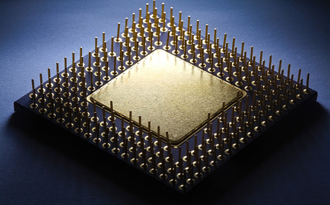
A CSP to BGA adapter links a chip-scale package (CSP) to a ball grid array (BGA) footprint. This lets a chip fit into a board that was not made for it. It’s a little like using a travel plug so your phone charger works in another country. It also helps when the CSP pins are too close together for normal PCB assembly, making the adapter a bridge between fine-pitch parts and standard layouts.
In a test lab, engineers might need to try a new chip on an older board before building a new one. The adapter makes this possible without redesigning everything. In large factories, adapters help add new parts to old lines, saving money on new tools. For example, in car electronics, an adapter can be used in early testing of an engine control chip before the final design is ready.
Breakout boards and sockets also connect chips, but adapters have a mix of strong mechanical hold and good electrical routing. Sockets can be handy if you want to keep swapping chips in and out, but they often cannot match the steady connection and signal quality of a soldered adapter.
With high-reliability devices, small mistakes can lead to big headaches.
If one solder ball is out of place, you can end up with a short or an open circuit. In fine-pitch designs, this risk is even higher. Some radar modules in aerospace work at such high speeds that a tiny misalignment can change the signal path just enough to cause errors.
Different materials expand at different rates when heated. If the adapter and PCB expand too differently, stress builds up in the joints, and over time cracks can form. DEEPETCH often uses ceramic for the adapter base, which stays stable even with big temperature swings, reducing the chance of failure.
In aircraft, cars, or heavy machines, parts are shaken, heated, and cooled again and again. A well-made adapter keeps its contacts firm despite all this stress. In aerospace testing, adapters have been put through vibration levels similar to rocket launches, and only those made to tight tolerances stayed in perfect working order.
Not all devices need the same quality. Your home game console may not need the same adapter as a satellite or a medical scanner. But some fields simply cannot afford a weak link.
In space or military systems, a failure can mean losing a mission. Once a satellite is in orbit, you cannot send someone to fix it. The adapter must handle vibration, vacuum, and extreme temperature shifts without losing function.
In a car engine bay or a factory floor, electronics are under constant stress. Parts must keep working for years despite heat, dust, and vibration. A cracked solder joint could stop an entire production line or disable safety features in a vehicle.
Hospitals and communication networks run around the clock. If a device fails, lives or essential services may be at risk. That’s why in these areas, adapters are often made to standards far above average.
Getting this level of precision is not luck—it takes the right design, tools, and checks at every stage.
Ceramic is a favorite here because it expands very little when heated and stays stable over time. DEEPETCH’s equipment is designed to work with ceramic substrates while holding alignment down to just a few microns, even after hundreds of heat cycles. It also offers customization options to meet your needs.
Machines with vision guidance and servo control place each chip exactly where it should be. The target is often ±5 μm, which is thinner than a strand of hair. The systems also check themselves during long runs, so accuracy does not drift as parts heat up or tools wear down.
Every adapter is inspected at several points—first visually, then for electrical continuity, and finally under mechanical stress. DEEPETCH’s certifications in aerospace, defense, and communications prove it can meet these tough, repeatable standards.
Precision does not just mean “better numbers” in a lab—it affects cost, reliability, and even project speed.
If each adapter is built right, you throw away fewer boards, save material, and keep the line moving. Small savings on waste can add up to big numbers over months of production.
Good adapters keep their electrical and mechanical properties for years. That means less downtime, fewer urgent repairs, and happier end users.
One adapter design can often work in different boards and setups. This makes it easier to shift from lab testing to mass production without starting from scratch.
Chips are not getting simpler, and adapters need to keep up.
New designs are packing more pins into smaller areas. This pushes adapter makers to be even more precise. Techniques like laser soldering may soon be more common to handle these tight spaces.
Future adapters may include built-in checks to help engineers spot problems during testing, which could save hours when working with large chip batches.
Developing new ceramics or composite materials could give adapters longer life, better moisture resistance, and higher shock tolerance, especially for outdoor or heavy-duty use.
Q1: What is the typical alignment tolerance for a high-precision CSP to BGA adapter
A: Around ±5 μm is common for top-end adapters, important for fine-pitch and high-speed designs.
Q2: How do adapters affect signal integrity in high-frequency applications
A: A well-designed adapter keeps signal loss and unwanted reflections to a minimum by maintaining steady routing.
Q3: Are these adapters reusable for different testing phases
A: Many can be reused if they are handled with care and checked for wear or dirt before each use.

The DE-CW-1310 DFB EPI wafer, a high-performance epitaxial structure designed for distributed feedback (DFB) lasers operating at 1310 nm....

Ceramic thin-filmvacuum sensor Optical gas massflowmeter Liquid mass flowmeter Force sensor MEMS...

Photoelectric sensing chip Light source chips Optical transmission and modulationchips Optical detection and receptionchips...

Using a“Detach Core”which has two-layers carrier foil structure on the surface as a core, and forming...

Tenting process is a kind of subtractive process, the process as follows: Laminating photosensitive film...

Modified Semi-Added Process abbreviated as mSAP, which can be used on the core or build-up layers, pattern...

Semi-Added Process abbreviated as SAP, using on the build-up-layer pattern forming as follow:First depositing...

The product generally adopts the pressing lamination process of semi-curing sheets , and line formation...

The products generally adopt the Build-up Film Lamination process, and the circuit formation uses the...

Equipment features: 1. Non-destructive precision testing Micrometer-level probe contact technology...