

Silicon On Insulators (Soi)

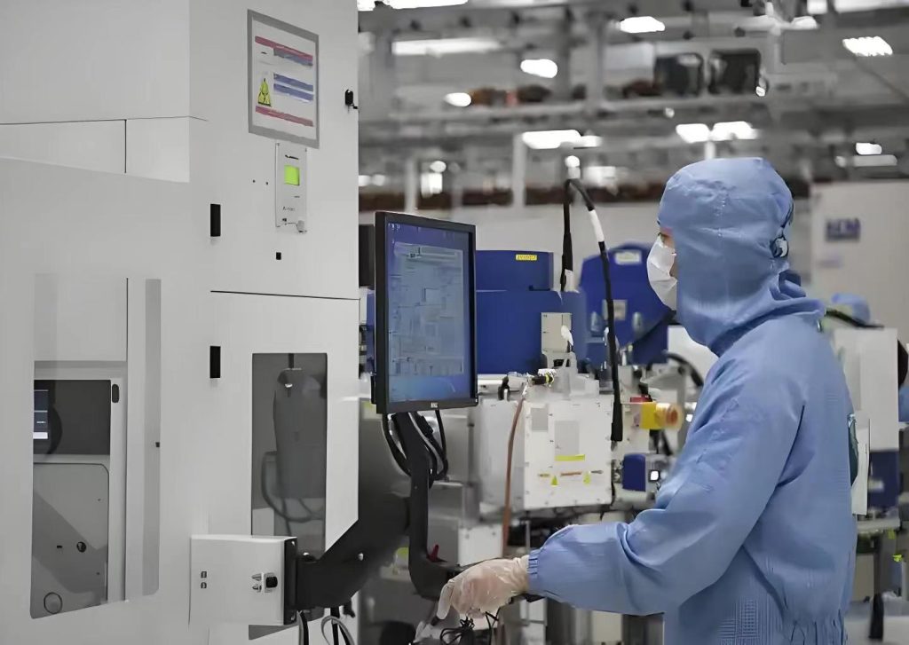
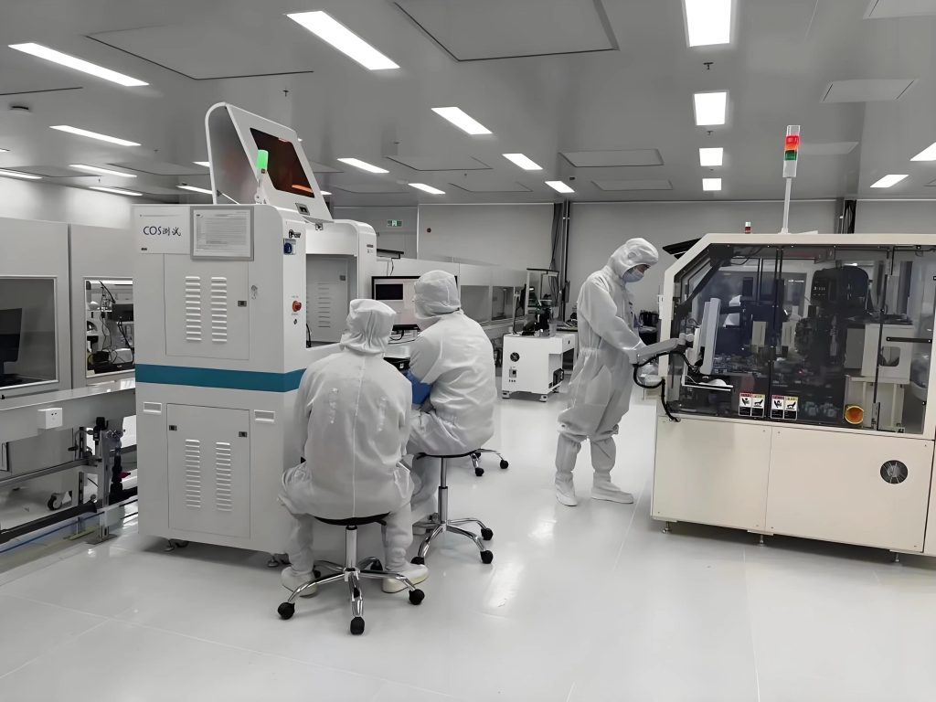
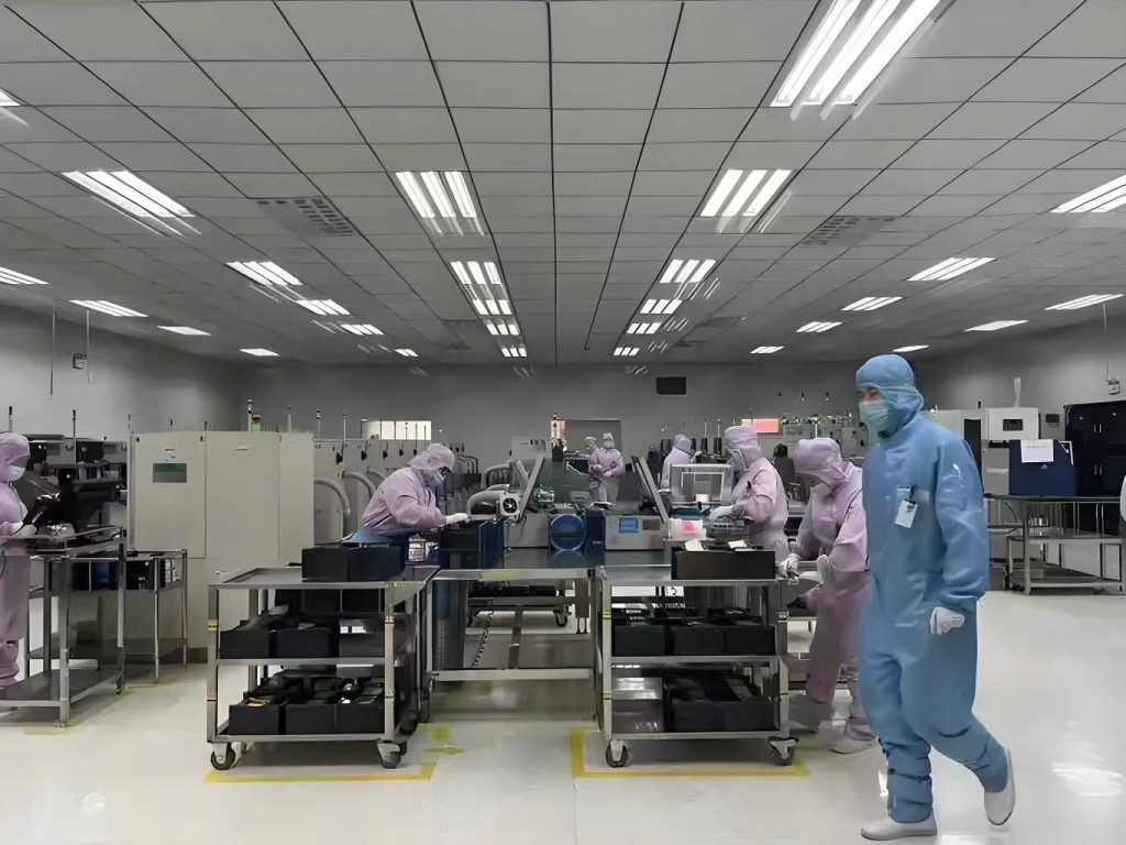
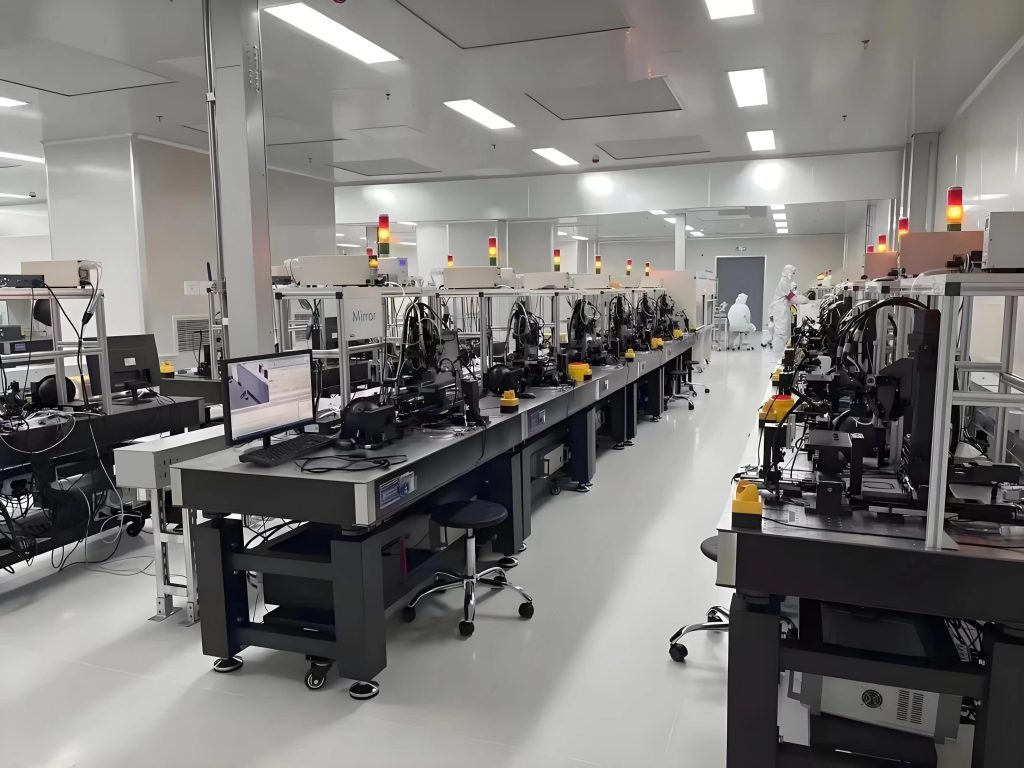
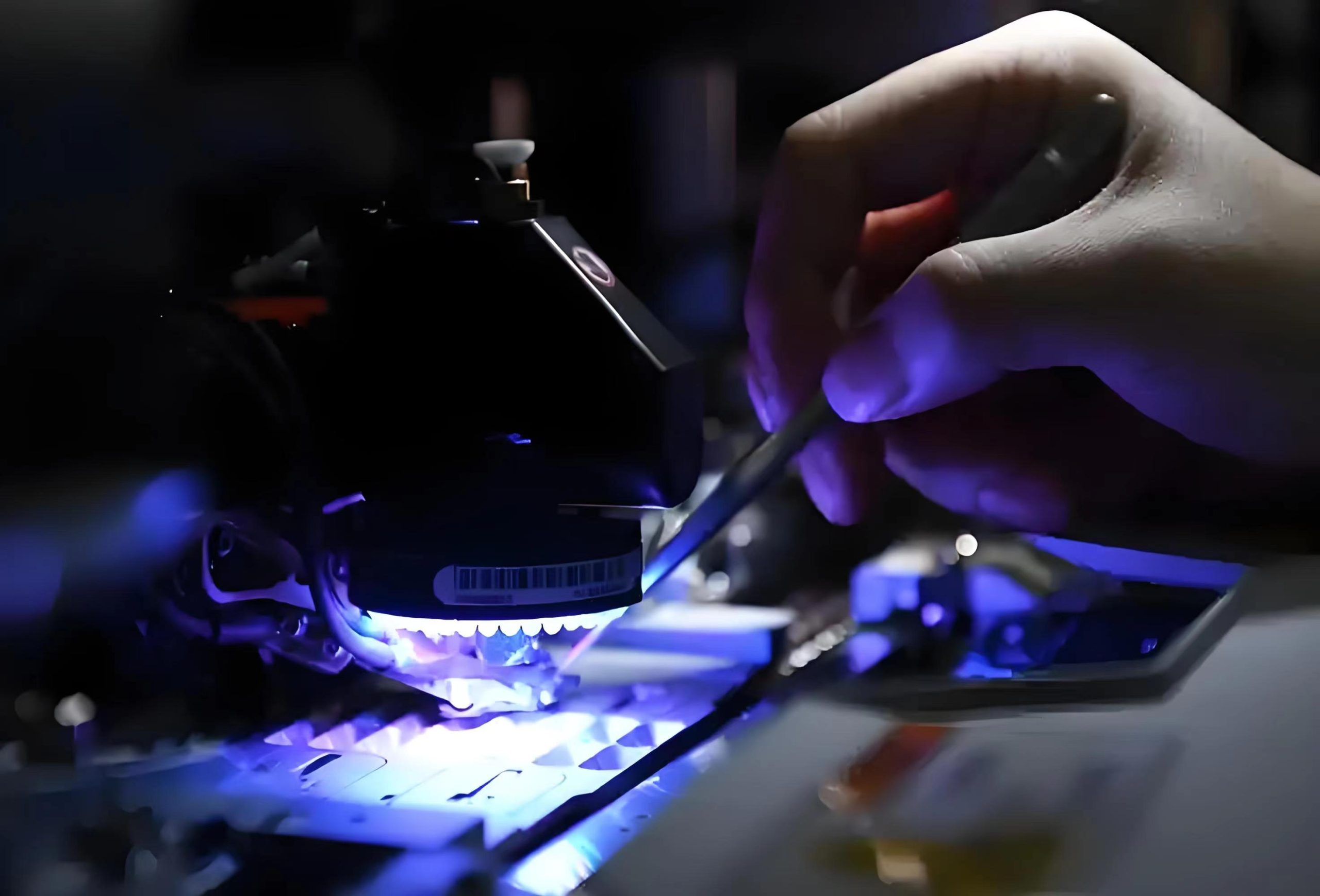
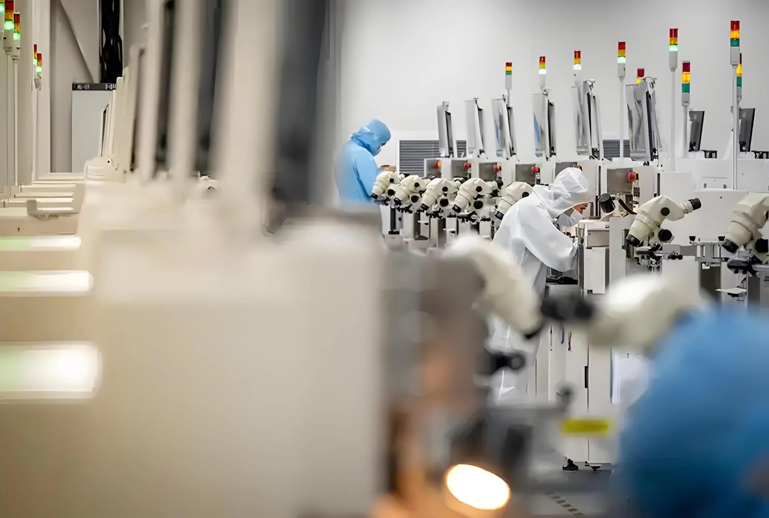
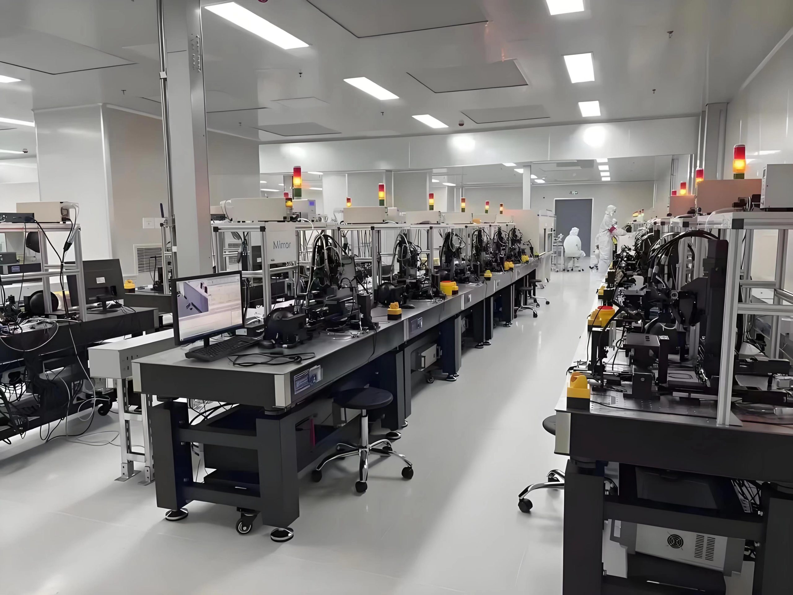
Product album display

Application Areas

  • SOI’s industry applications
  1. High voltage and power devices

IGBT and MOSFET: buried oxygen layer isolation for high voltage (>1200 V) and reduced on-state resistance.

Automotive electronics: used in engine control units (ECUs) and battery management systems (BMS), with tolerance to extreme temperatures of-40℃ to 150℃.

  1. RF and microwave devices

Radio frequency front end (RF-SOI): Used for 5G millimeter wave RF switches (such as SKYWORKS’S SKY5® series), insertion loss <0.5 DB

5G chip: SOI’s low parasitic capacitance and high cutoff frequency (FT>200 GHZ) improve signal transmission efficiency.

Millimeter wave radar: used for 77 GHZ vehicle-mounted radar chip to reduce signal loss.

Low-power processors: IBM’s POWER server chips use SOI technology to improve energy efficiency by 40%

  1. Sensor MEMS

Pressure sensor: the insulation of the buried oxygen layer is used to achieve high sensitivity and anti-interference ability.

Micro accelerometer: The mechanical stability of SOI supports high precision inertial measurement.

Gyro: SOI technology is used in MEMS gyroscopes to improve accuracy and stability

  1. Anti-radiation electronic equipment

Aerospace: The buried oxygen layer reduces the charge accumulation caused by ionizing radiation and improves the ability to resist single particle flip (SEU).

  1. High performance integrated circuits

Microprocessors: SOI technology is used in high-performance microprocessors to improve speed and reduce power consumption.

Quantum bits: Spin quantum bits of silicon in SOI structure, with decoherence time extended to more than 1 second

IDM Customization Service

From advanced processes to specialty processes, we use our IDM vertical integration experience to help customers overcome design-process collaboration challenges.

01

Supports advanced nodes such as [5-22nm FinFET/BCD/GAA] to meet the needs of high-performance computing (HPC), AI chips, etc.

02

MPW (Multi-Project Wafer) Service: Small batch trial production to reduce customers' initial costs. Customized process development: Cooperate with customers to conduct DTCO (Design-Process Co-Optimization), customize design rules and process parameters.

03

We support the joint solution of "wafer foundry + advanced packaging" (such as 3D IC, heterogeneous integration) to avoid the loss of multi-supplier collaboration. Unlike pure foundries, we verify the process stability through mass production of our own chips to reduce the risk of tape-out for you.

Provide customers with complete integrated manufacturing services from concept to finished product

01

Electronic manufacturing services and printed circuit board assembly.

02

EMS provides a wide range of electronic manufacturing services, including everything from circuit board design to supply chain management to assembly, testing and after-sales support.

03

PCBA is a link in EMS that focuses on the assembly of printed circuit boards, covering component placement, soldering and related testing, connecting electronic components to manufactured printed circuit boards.

News Center