
FCBGA(Flip Chip Ball Grid Array)Due to its high-density interconnection, excellent heat dissipation and electrical characteristics, packaging substrates are widely used in the following fields with high requirements for performance, reliability and integration.
1. High-performance computing: CPU, GPU, FPGA and other high-performance chips.
2.Artificial intelligence and machine learning: AI accelerators (such as TPU, NPU), deep learning chips. Heat dissipation capacity can cope with long-term high-load computing.
3.Network and Communications: 5G base station chips, high-speed switches/routers, optical modules.
4.Automotive electronics: autonomous driving chips, ADAS controllers, and in-vehicle infotainment systems.
5.Data center and server: server CPU, memory controller, PCIe accelerator card.
6.Consumer electronics: game console SoC, high-end laptops, AR/VR devices. Support high-performance integration in a limited space, balance power consumption and heat dissipation, and improve user experience.
7.Industrial and medical equipment: industrial automation controllers, medical imaging equipment (such as MRI, CT).
8.Military and aerospace: radar systems, satellite communications, missile guidance. The extreme temperature resistance and radiation resistance design meet military standards (MIL-STD-883) to ensure the reliability of equipment under extreme conditions.
Diamond-Copper Thermally Conductive Composite. High thermal conductivity, tunable CTE, robust.

The DE-CW-1310 DFB EPI wafer, a high-performance epitaxial structure designed for distributed feedback (DFB) lasers operating at 1310 nm....

Ceramic thin-filmvacuum sensor Optical gas massflowmeter Liquid mass flowmeter Force sensor MEMS...

Photoelectric sensing chip Light source chips Optical transmission and modulationchips Optical detection and receptionchips...

Using a“Detach Core”which has two-layers carrier foil structure on the surface as a core, and forming...

Tenting process is a kind of subtractive process, the process as follows: Laminating photosensitive film...

Modified Semi-Added Process abbreviated as mSAP, which can be used on the core or build-up layers, pattern...

Semi-Added Process abbreviated as SAP, using on the build-up-layer pattern forming as follow:First depositing...

The product generally adopts the pressing lamination process of semi-curing sheets , and line formation...
The products generally adopt the Build-up Film Lamination process, and the circuit formation uses the...
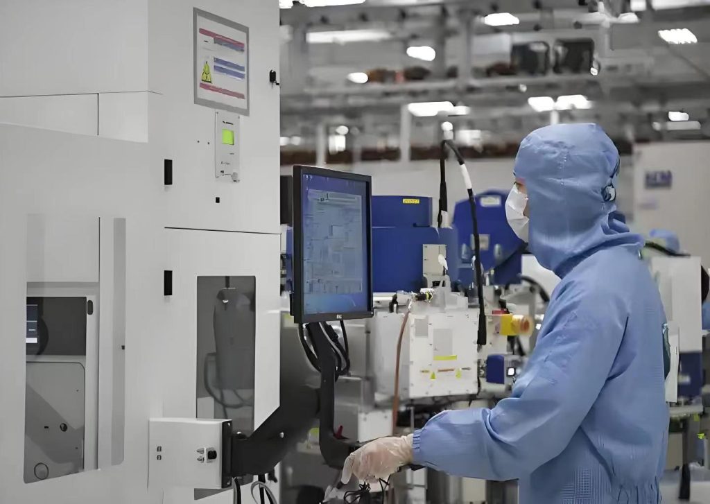
Supports advanced nodes such as [5-22nm FinFET/BCD/GAA] to meet the needs of high-performance computing (HPC), AI chips, etc.
MPW (Multi-Project Wafer) Service: Small batch trial production to reduce customers' initial costs. Customized process development: Cooperate with customers to conduct DTCO (Design-Process Co-Optimization), customize design rules and process parameters.
We support the joint solution of "wafer foundry + advanced packaging" (such as 3D IC, heterogeneous integration) to avoid the loss of multi-supplier collaboration. Unlike pure foundries, we verify the process stability through mass production of our own chips to reduce the risk of tape-out for you.
Electronic manufacturing services and printed circuit board assembly.
EMS provides a wide range of electronic manufacturing services, including everything from circuit board design to supply chain management to assembly, testing and after-sales support.
PCBA is a link in EMS that focuses on the assembly of printed circuit boards, covering component placement, soldering and related testing, connecting electronic components to manufactured printed circuit boards.
Title: Semiconductor manufacturing processes Objective: To have a certain foundation for the overall...