

Diamond

Product album display

Application Areas

  • Industry applications
  1. High frequency communication and 5G/6G

RF power amplifier: used in 5G base stations and millimeter wave radar, supporting higher frequency bands (24-100 GHZ) and low signal loss.

Optical communication module: diamond photoelectric detector improves the optical fiber communication rate to 800G level.

Field-effect transistor (FET): Cut-off frequency (Fₜ) exceeds 100 GHZ, suitable for 5G millimeter-wave base stations and satellite communications.

Terahertz (THZ) devices: THZ emitters and detectors are developed using high carrier velocity (saturation velocity 2.7 x 10⁷ CM/S)

  1. New energy vehicles and power electronics

Power devices: Diamond-based MOSFET and IGBT can reduce the loss of electric vehicle inverter, shorten the charging time, and improve the battery life.

Heat dissipation system: integrated diamond microchannel heat dissipation module, so that the junction temperature of GAN device is reduced from 676℃ to 182℃.

  1. Extreme environment and cutting-edge technology

Aerospace: High temperature and high pressure characteristics are suitable for rocket engine sensors and satellite electronic systems.

Quantum computing: Diamond is used as a solid state carrier, and the nitrogen vacancy center (NV color center) in diamond can realize the efficient storage and processing of optical quantum states.

  1. Consumer electronics

Mobile phone / GPU cooling: The diamond cooling GPU tested by Nvidia can increase AI performance by three times; Huawei Diamond chip cooling patent layout

  1. High power electronic devices

Thyristor and IGBT: power conversion for electric vehicles and smart grid, achieving low on-resistance (<1 MΩ·CM²) and high switching frequency (> 100 KHZ).

Schottky diode: reverse breakdown voltage up to 5000 V, forward current density>100 A/CM²

  1. Optical devices

Deep ultraviolet detector: response wavelength <260 NM, used for flame monitoring and biomedical imaging.

Diamond laser: room temperature single photon emission is achieved through nitrogen vacancy (NV) color center to promote quantum communication.

  1. Package substrate

Diamond’s high thermal conductivity makes it a high-performance packaging substrate material, which can effectively reduce the temperature of electronic devices


IDM Customization Service

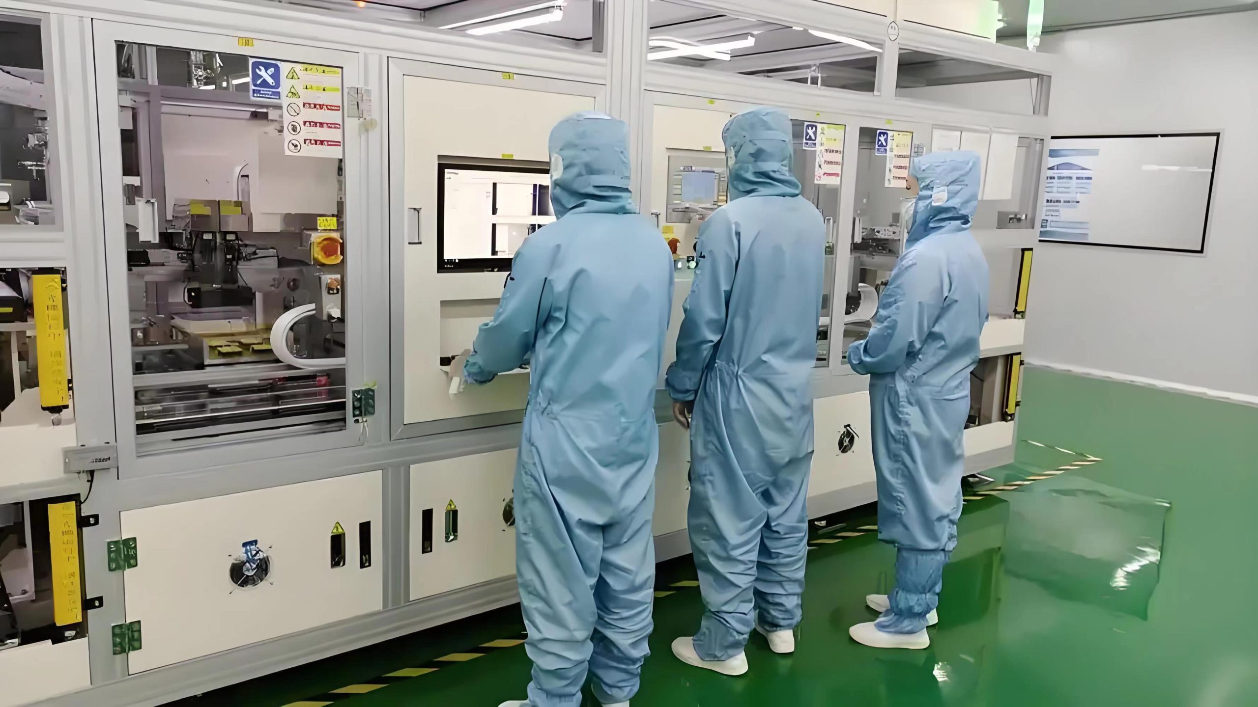
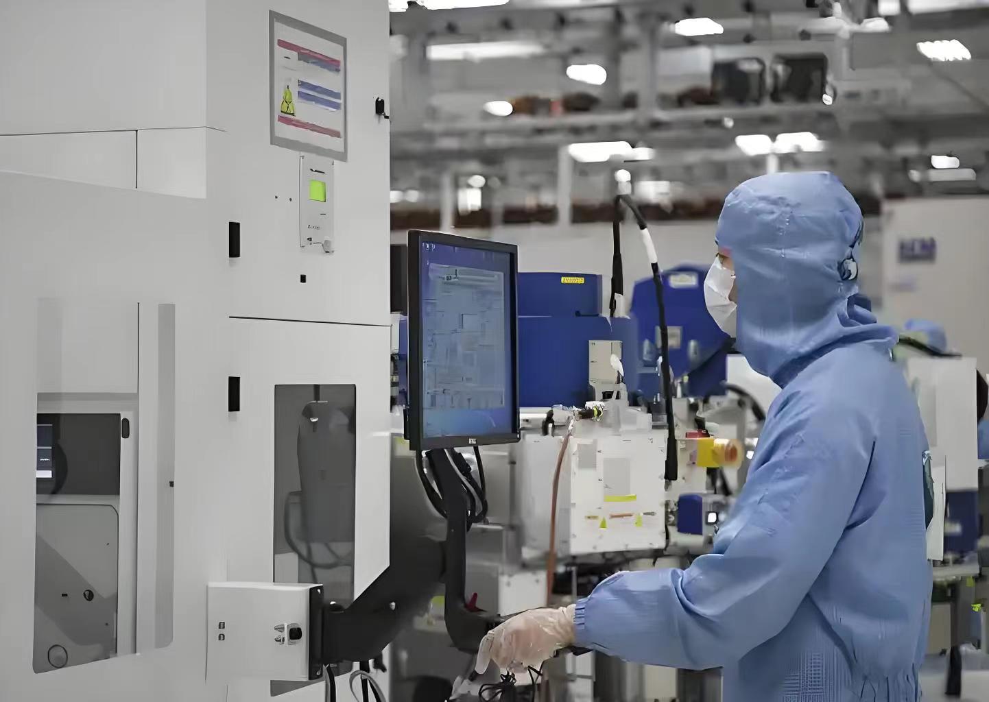
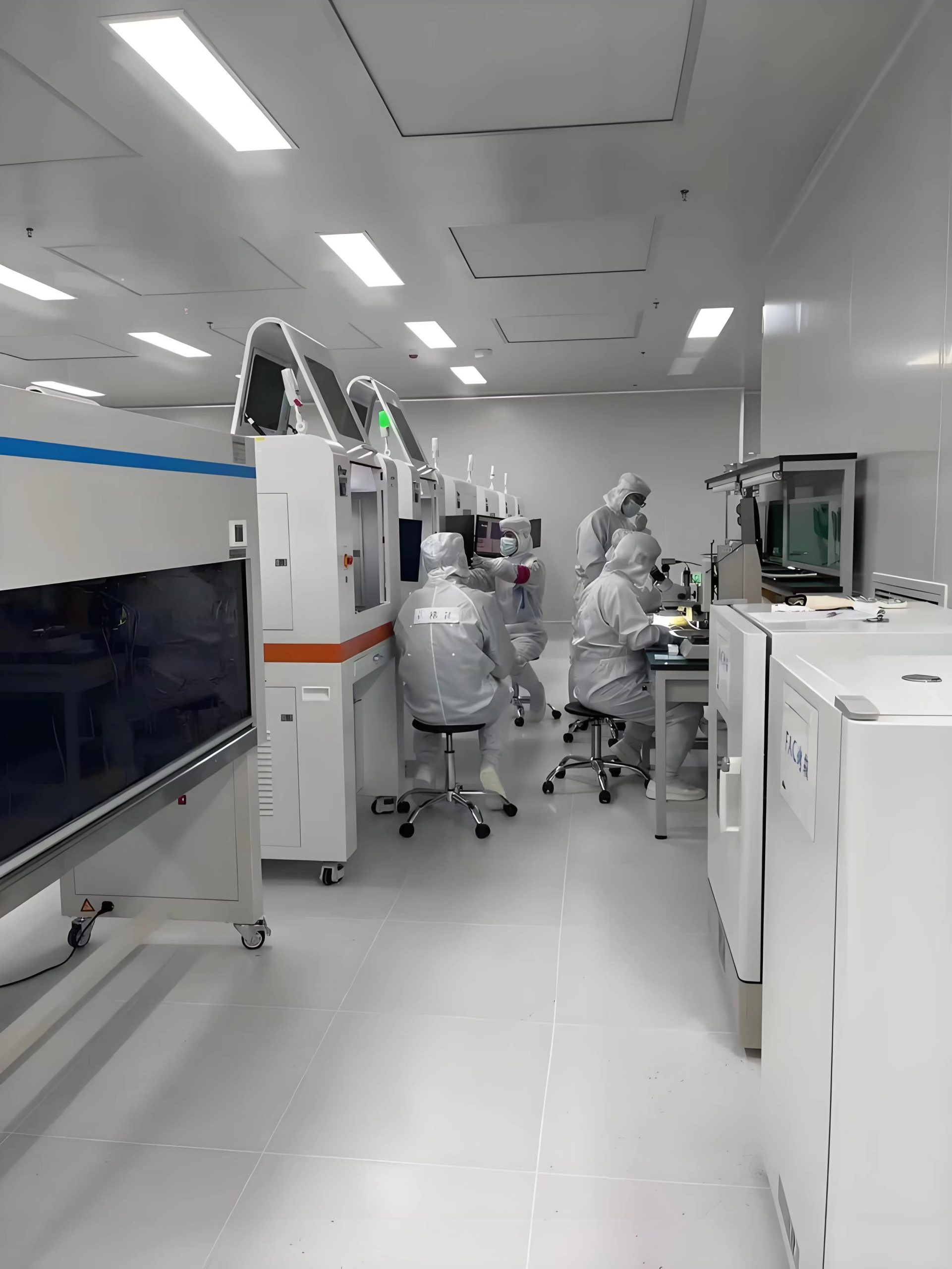
From advanced processes to specialty processes, we use our IDM vertical integration experience to help customers overcome design-process collaboration challenges.

01

Supports advanced nodes such as [5-22nm FinFET/BCD/GAA] to meet the needs of high-performance computing (HPC), AI chips, etc.

02

MPW (Multi-Project Wafer) Service: Small batch trial production to reduce customers' initial costs. Customized process development: Cooperate with customers to conduct DTCO (Design-Process Co-Optimization), customize design rules and process parameters.

03

We support the joint solution of "wafer foundry + advanced packaging" (such as 3D IC, heterogeneous integration) to avoid the loss of multi-supplier collaboration. Unlike pure foundries, we verify the process stability through mass production of our own chips to reduce the risk of tape-out for you.

Provide customers with complete integrated manufacturing services from concept to finished product

01

Electronic manufacturing services and printed circuit board assembly.

02

EMS provides a wide range of electronic manufacturing services, including everything from circuit board design to supply chain management to assembly, testing and after-sales support.

03

PCBA is a link in EMS that focuses on the assembly of printed circuit boards, covering component placement, soldering and related testing, connecting electronic components to manufactured printed circuit boards.

News Center