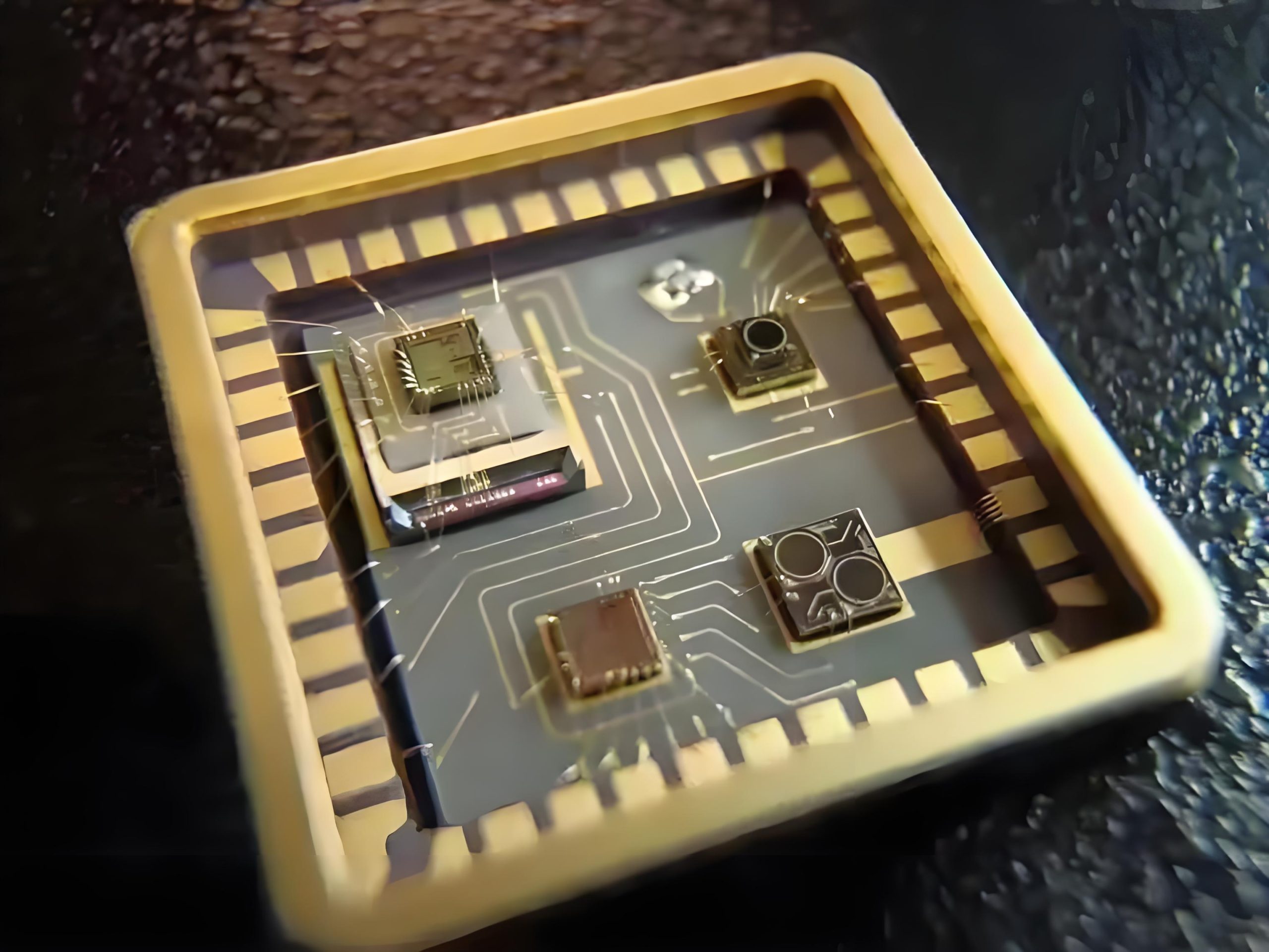


Indium phosphide (InP)

Product album display

Application Areas

  • Core application areas of indium phosphide
  1. Optical communication and laser technology

1550 NM laser: the core light source of optical fiber communication backbone network and 5G pretransmission network, supporting single-mode output power>100 MW. It can be used to manufacture various optoelectronic devices with high photoelectric conversion efficiency and high sensitivity, suitable for optical fiber communication system and optical display technology.

Quantum computing and lasers: Indium phosphide quantum dots have adjustable emission wavelengths suitable for quantum communication and quantum computing, and narrow linewidth (<100 KHZ) characteristics are suitable for quantum communication and optical communication systems

Optical communication field: mainly used to manufacture optical module devices, such as semiconductor lasers, optical detectors, etc. Support high-speed, large-capacity data transmission.

  1. High frequency electronic devices

Terahertz imaging and communication: INP-based HEMT and RTD (resonant tunneling diode) can generate and detect 0.3-3 THZ signals for security imaging and 6G ultra-high-speed wireless communication.

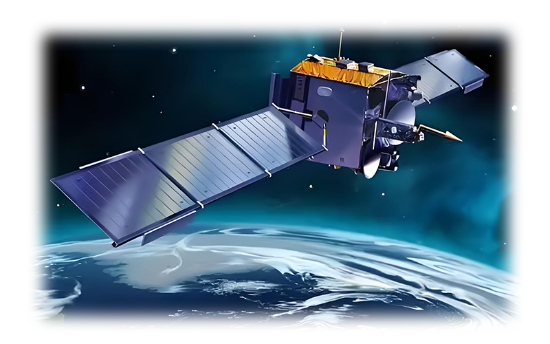
Millimeter wave integrated circuits: power amplifier chips for vehicle-mounted radar (77 GHZ) and satellite communications (KA band).

High frequency and high speed applications: High electron mobility (3000-4500 CM²/ (V·S) and high saturation electron drift velocity make it advantageous in the manufacturing of RF devices, suitable for the production of high-end RF devices, RF power amplifiers, high-frequency oscillators, etc., widely used in radar, satellite communication and other fields.

Sensors: Sensors made of indium phosphide have high sensitivity and high precision, suitable for biomedical signal detection and environmental monitoring in wearable devices, medical devices and other fields.


  1. Photoelectric detection and sensing

APD and PIN detectors: used in lidar (LIDAR) and fiber optic sensing systems with detection sensitivity of-30 DBM.

Gas sensor: The INP based photonic crystal sensor can detect trace gases (methane, CO₂) at the PPB level.

IDM Customization Service

From advanced processes to specialty processes, we use our IDM vertical integration experience to help customers overcome design-process collaboration challenges.

01

Supports advanced nodes such as [5-22nm FinFET/BCD/GAA] to meet the needs of high-performance computing (HPC), AI chips, etc.

02

MPW (Multi-Project Wafer) Service: Small batch trial production to reduce customers' initial costs. Customized process development: Cooperate with customers to conduct DTCO (Design-Process Co-Optimization), customize design rules and process parameters.

03

We support the joint solution of "wafer foundry + advanced packaging" (such as 3D IC, heterogeneous integration) to avoid the loss of multi-supplier collaboration. Unlike pure foundries, we verify the process stability through mass production of our own chips to reduce the risk of tape-out for you.

Provide customers with complete integrated manufacturing services from concept to finished product

01

Electronic manufacturing services and printed circuit board assembly.

02

EMS provides a wide range of electronic manufacturing services, including everything from circuit board design to supply chain management to assembly, testing and after-sales support.

03

PCBA is a link in EMS that focuses on the assembly of printed circuit boards, covering component placement, soldering and related testing, connecting electronic components to manufactured printed circuit boards.

News Center