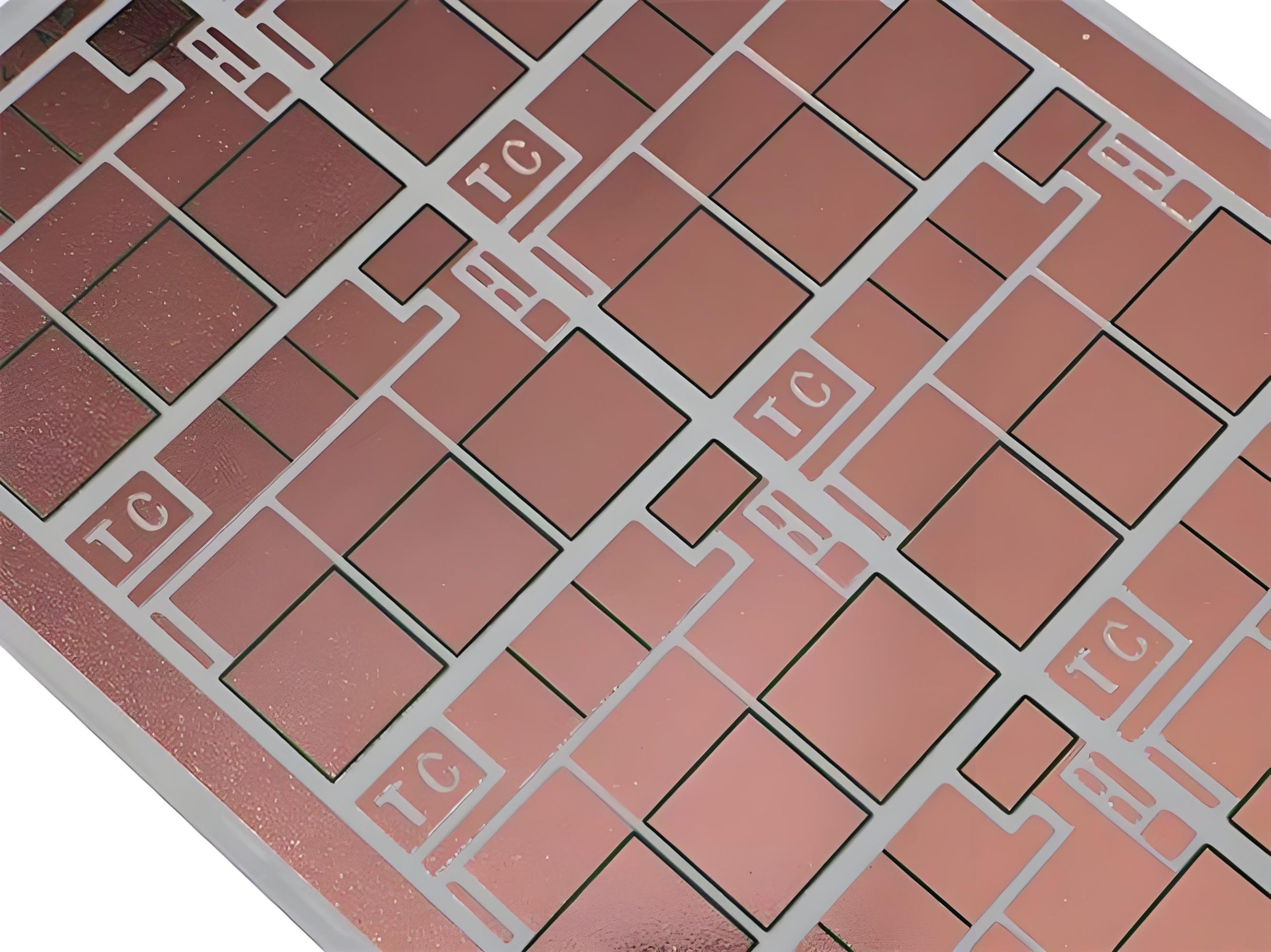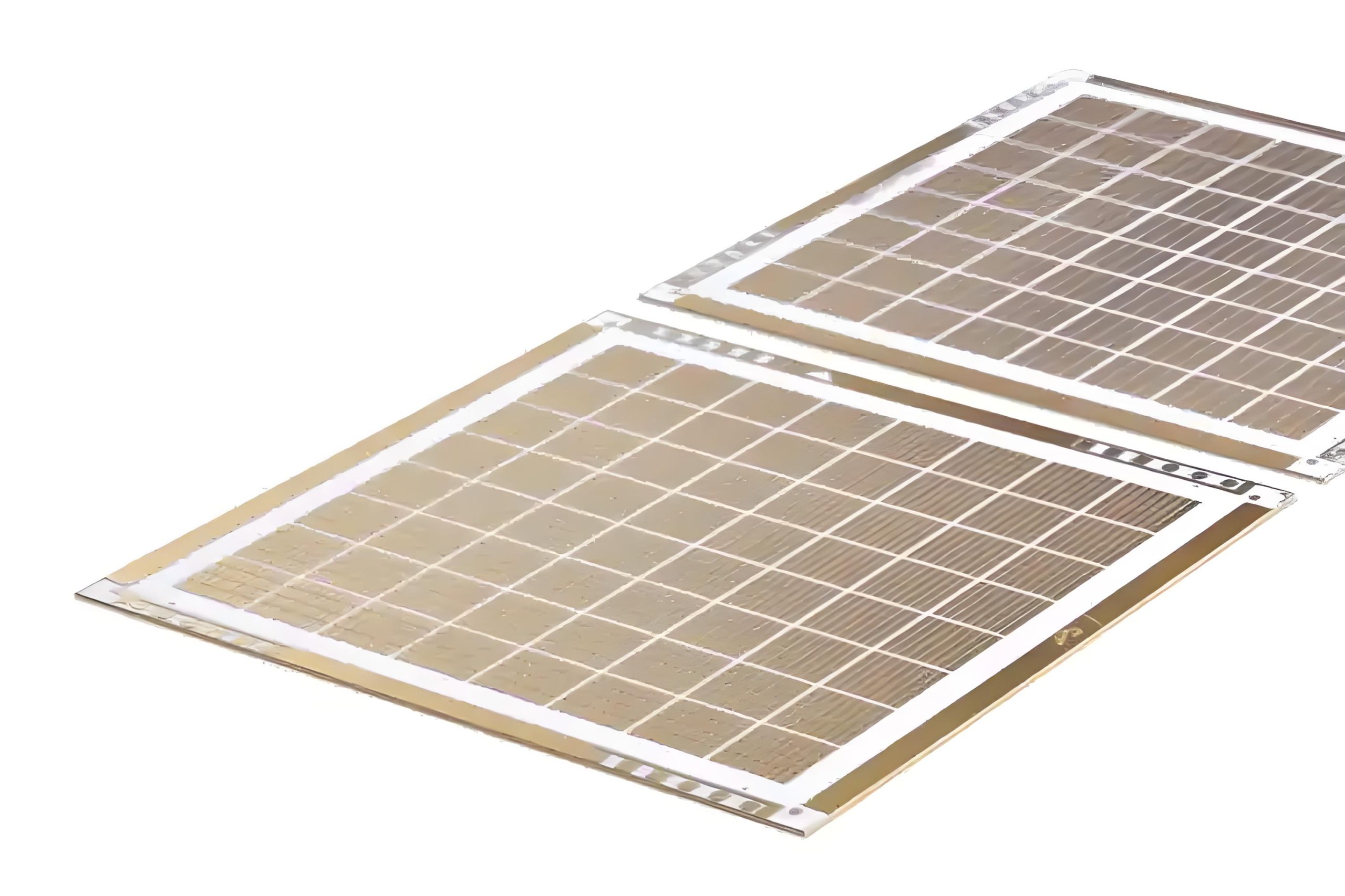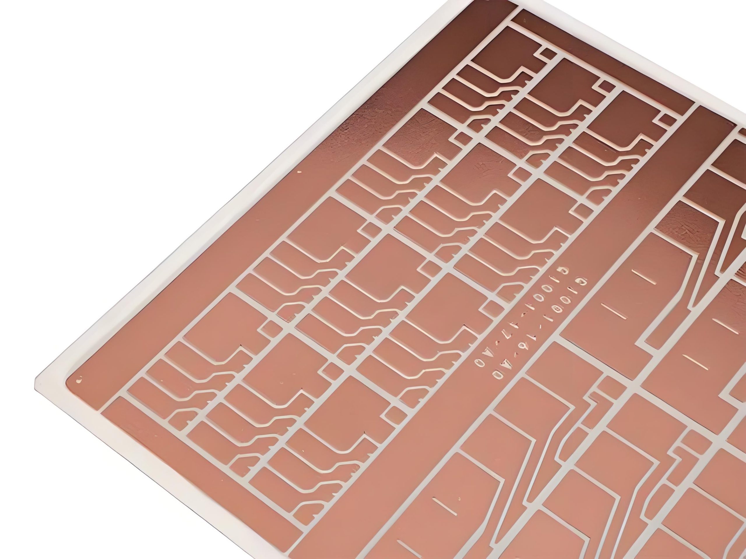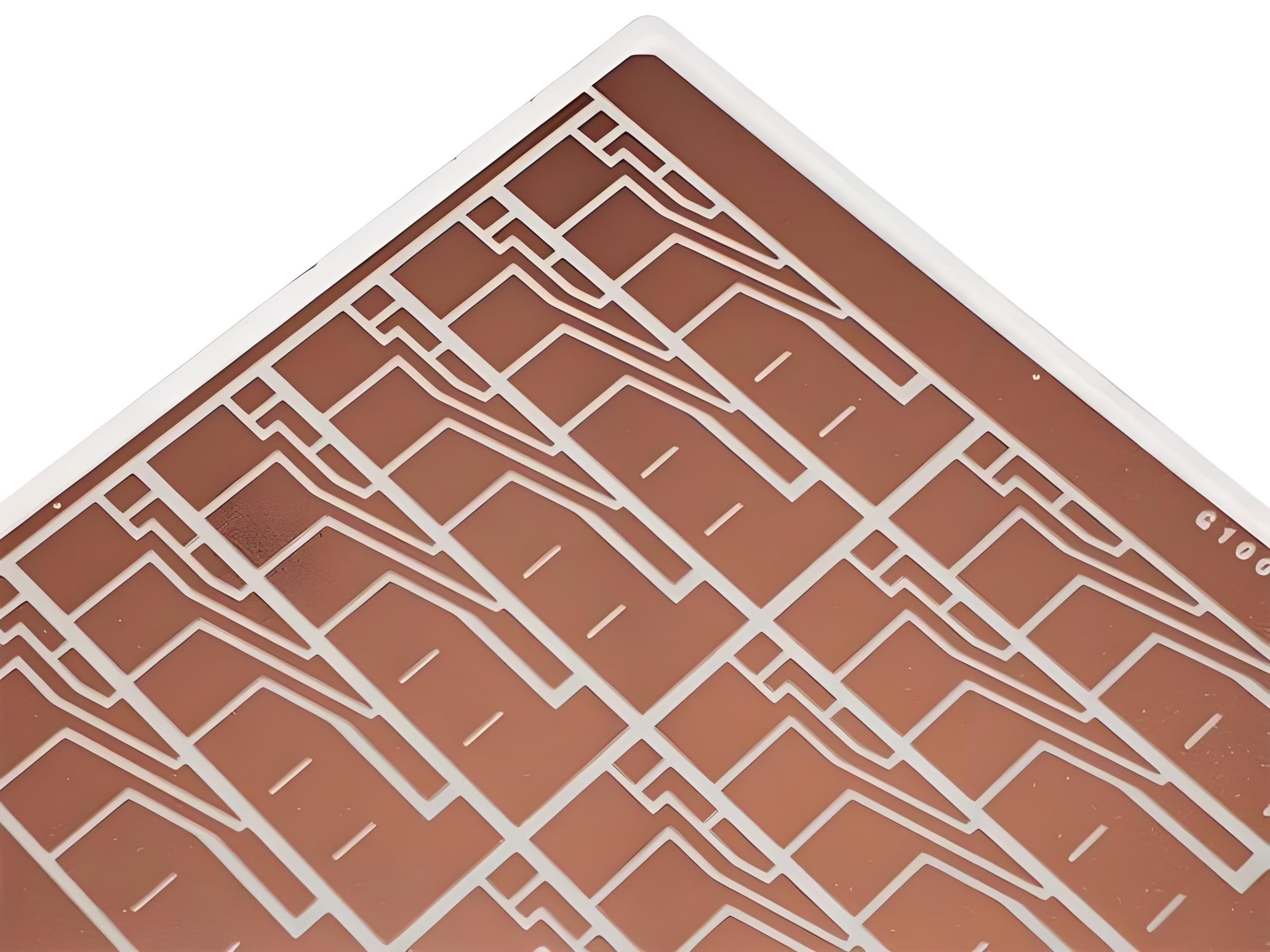

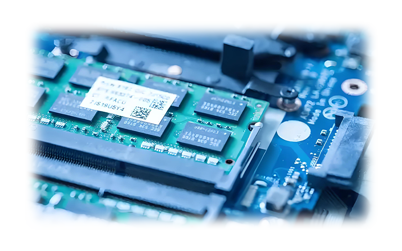
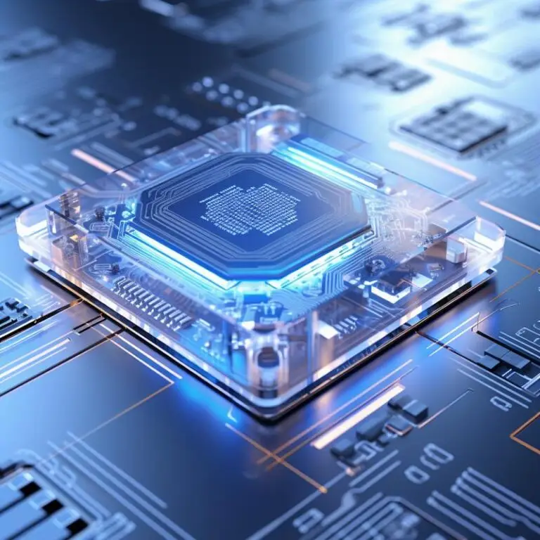
IGBT module: alumina ceramic substrate is used as the insulating substrate of power module to improve heat dissipation performance and reliability.
MOSFET Module: alumina ceramic substrate is used for the packaging of high frequency power devices.
It is superior to FR-4 substrate (thermal conductivity <0.3 W/ (M·K)), supports IGBT/MOSFET heat dissipation, and the operating temperature can reach 300℃.
LED substrate: Alumina ceramic substrate is used for the packaging of LED chips to improve heat dissipation performance and life, which is 50% lower than that of aluminum nitride (thermal conductivity 200+ W/ (M·K)), meeting the needs of general lighting; light efficiency is improved by 15%, and the life is>50,000 hours.
The dielectric loss (TANΔ<0.0002) is lower than that of plastic substrate and is suitable for 5G millimeter wave band.
The humidity resistance (85℃/85% RH) test is greater than 1000 hours through the AEC-Q200 certification.
Radiation resistance: anti Γ ray> 100 KGY, used in satellite power system.
The SCH Series is a high-performance DAF/DDAF (Die Attach Film) designed to streamline and enhance the advanced packaging process....
The DEEPETCH DP-QPA2611 is a high-performance X-Band (8–12 GHz) Gallium Nitride (GaN) Power Amplifier...
The DEEPETCH DP-ROS-40121 is a premium, solvent-free epoxy die attach adhesive engineered for the most...
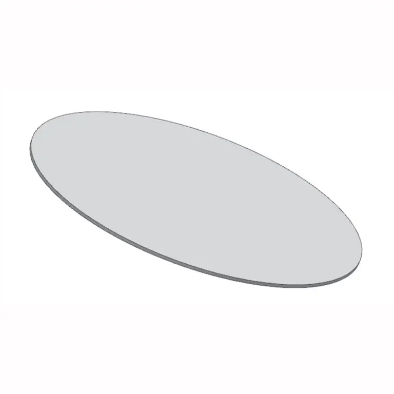
The Diamond Heat Spreader is a highly efficient thermal management material engineered for the most demanding...
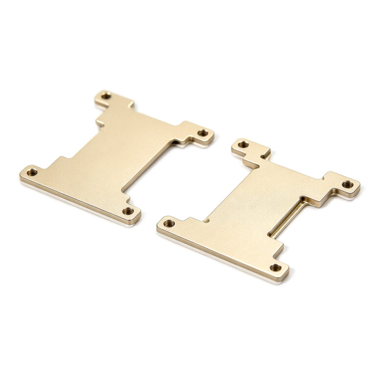
Molybdenum copper composite: adjustable CTE, high conductivity, lower density than tungsten copper. No...
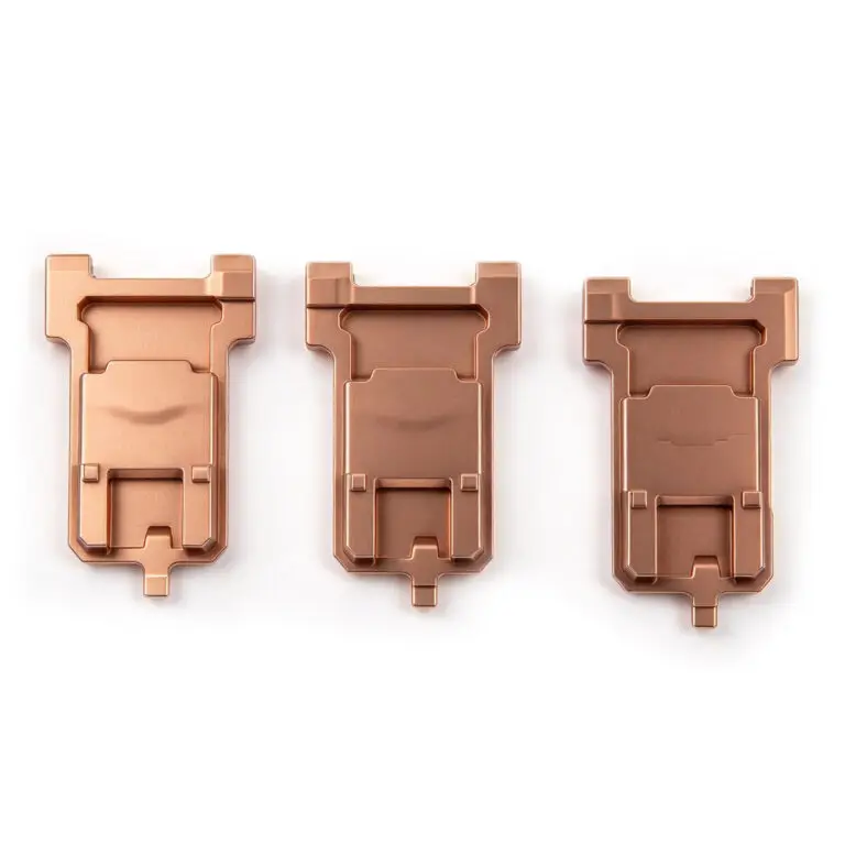
Tungsten copper composite: low CTE, high conductivity. Ideal for RF, power, optical packaging.
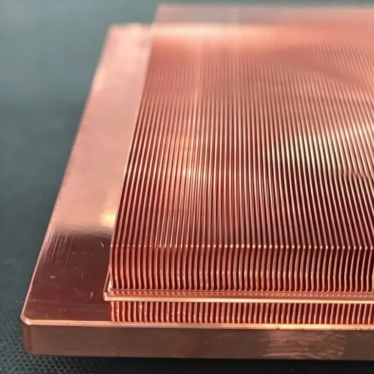
Diamond-Copper Thermally Conductive Composite. High thermal conductivity, tunable CTE, robust.
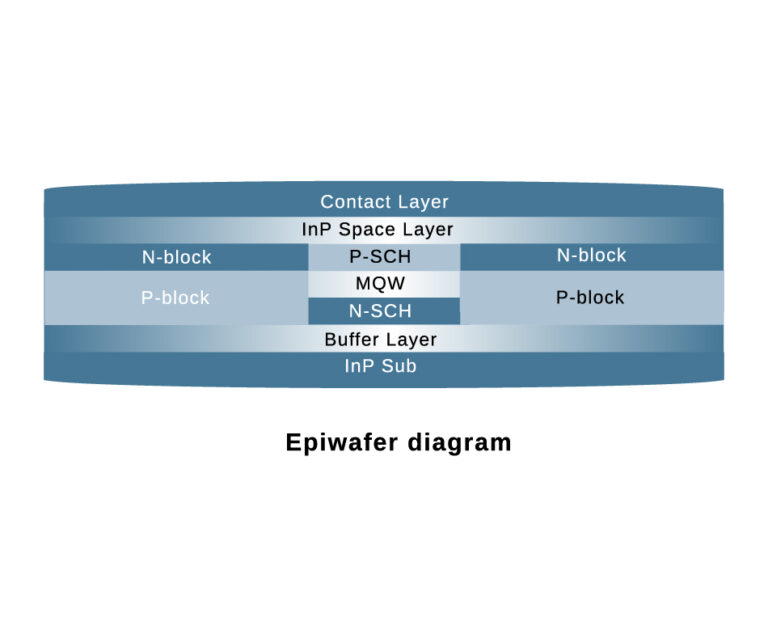
The DE-CW-1310 DFB EPI wafer, a high-performance epitaxial structure designed for distributed feedback (DFB) lasers operating at 1310 nm....
Ceramic thin-filmvacuum sensor Optical gas massflowmeter Liquid mass flowmeter Force sensor MEMS...
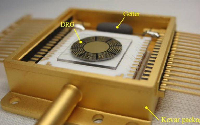
Photoelectric sensing chip Light source chips Optical transmission and modulationchips Optical detection and receptionchips...
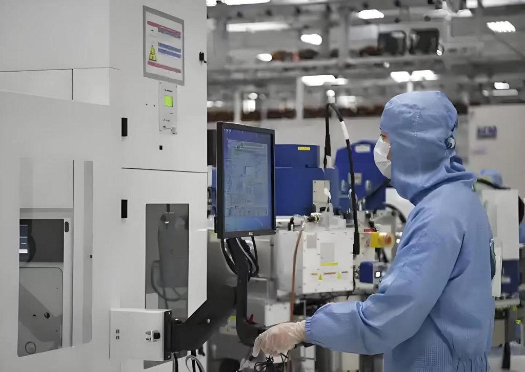
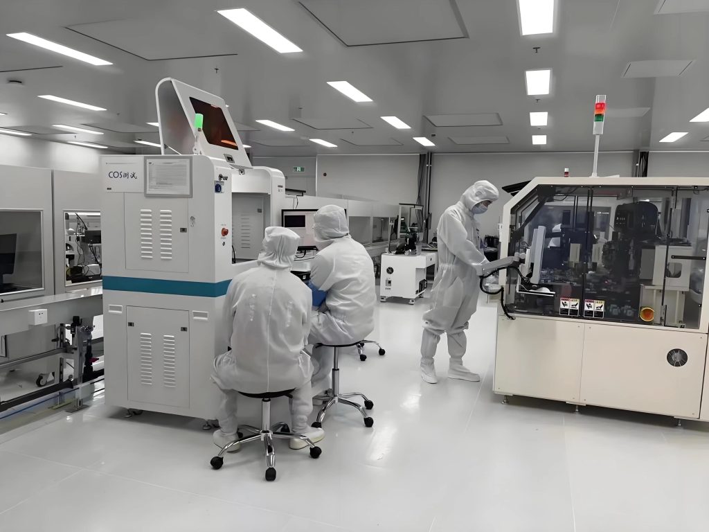
Supports advanced nodes such as [5-22nm FinFET/BCD/GAA] to meet the needs of high-performance computing (HPC), AI chips, etc.
MPW (Multi-Project Wafer) Service: Small batch trial production to reduce customers' initial costs. Customized process development: Cooperate with customers to conduct DTCO (Design-Process Co-Optimization), customize design rules and process parameters.
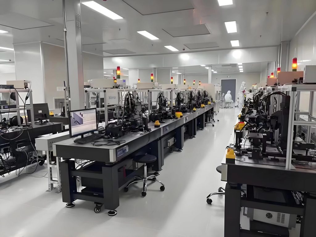
We support the joint solution of "wafer foundry + advanced packaging" (such as 3D IC, heterogeneous integration) to avoid the loss of multi-supplier collaboration. Unlike pure foundries, we verify the process stability through mass production of our own chips to reduce the risk of tape-out for you.
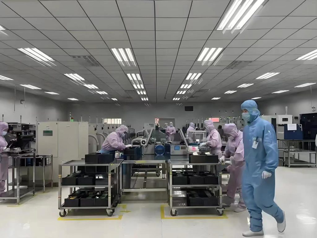
Electronic manufacturing services and printed circuit board assembly.
EMS provides a wide range of electronic manufacturing services, including everything from circuit board design to supply chain management to assembly, testing and after-sales support.
PCBA is a link in EMS that focuses on the assembly of printed circuit boards, covering component placement, soldering and related testing, connecting electronic components to manufactured printed circuit boards.
Title: Semiconductor manufacturing processes Objective: To have a certain foundation for the overall...