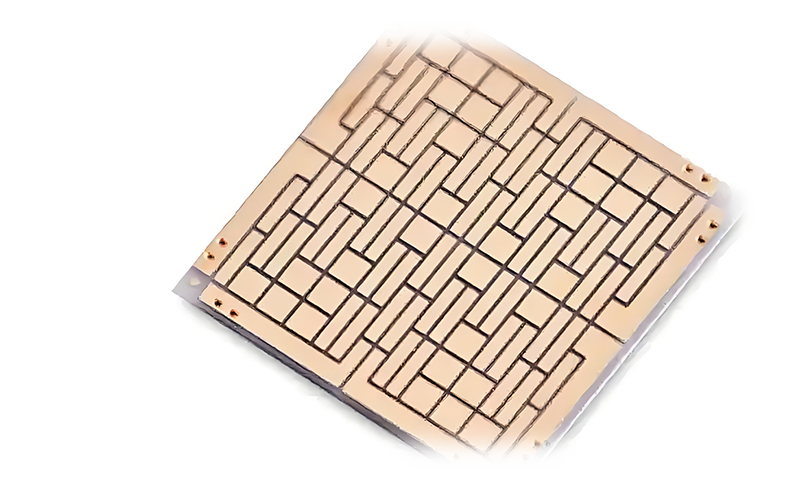


Cadmium Telluride (CdTe)

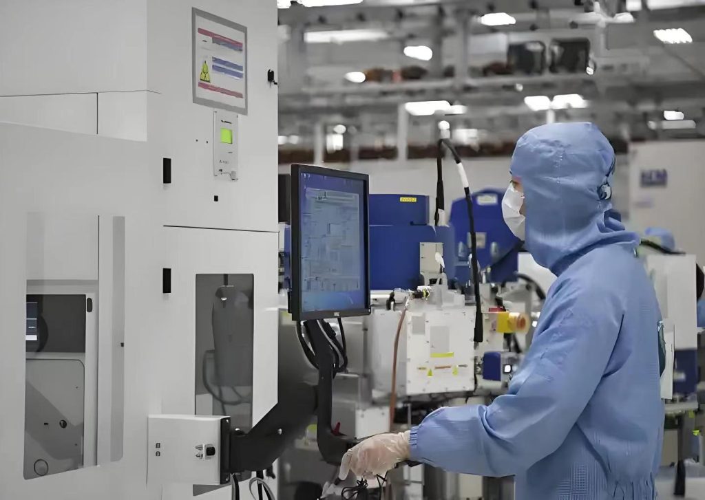
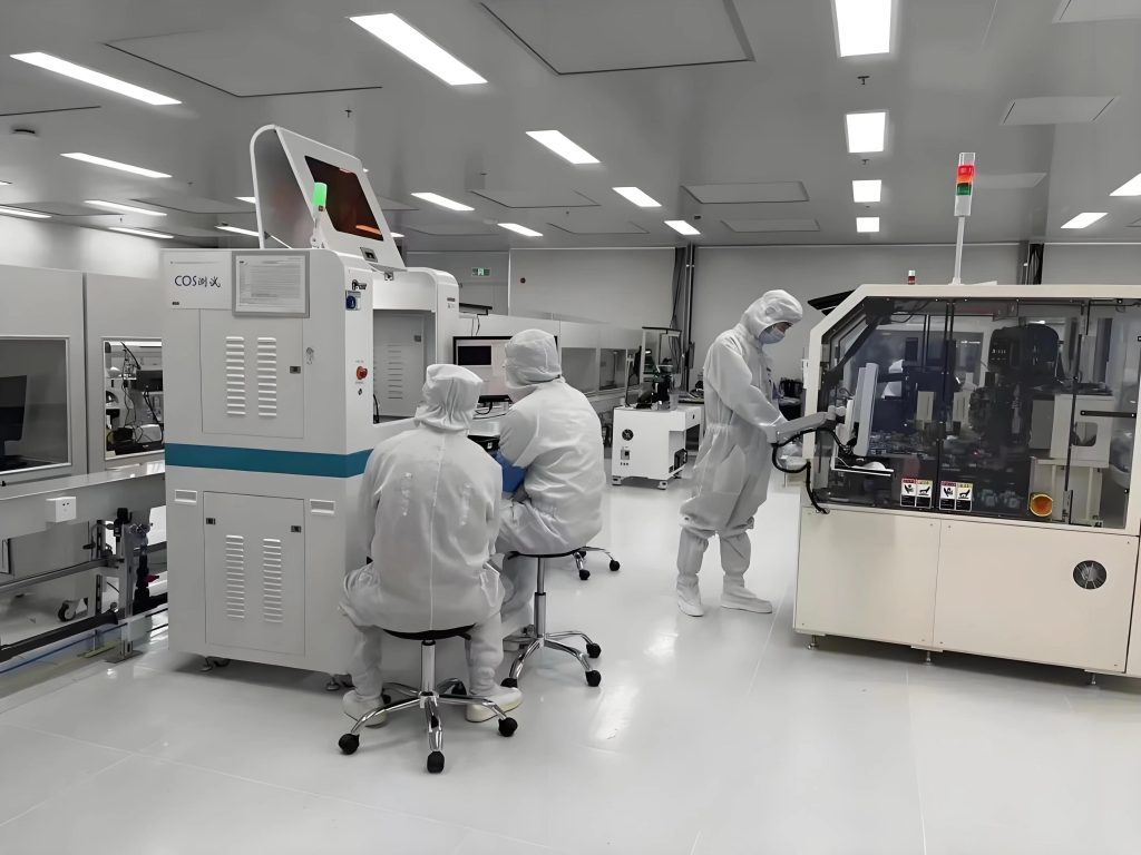
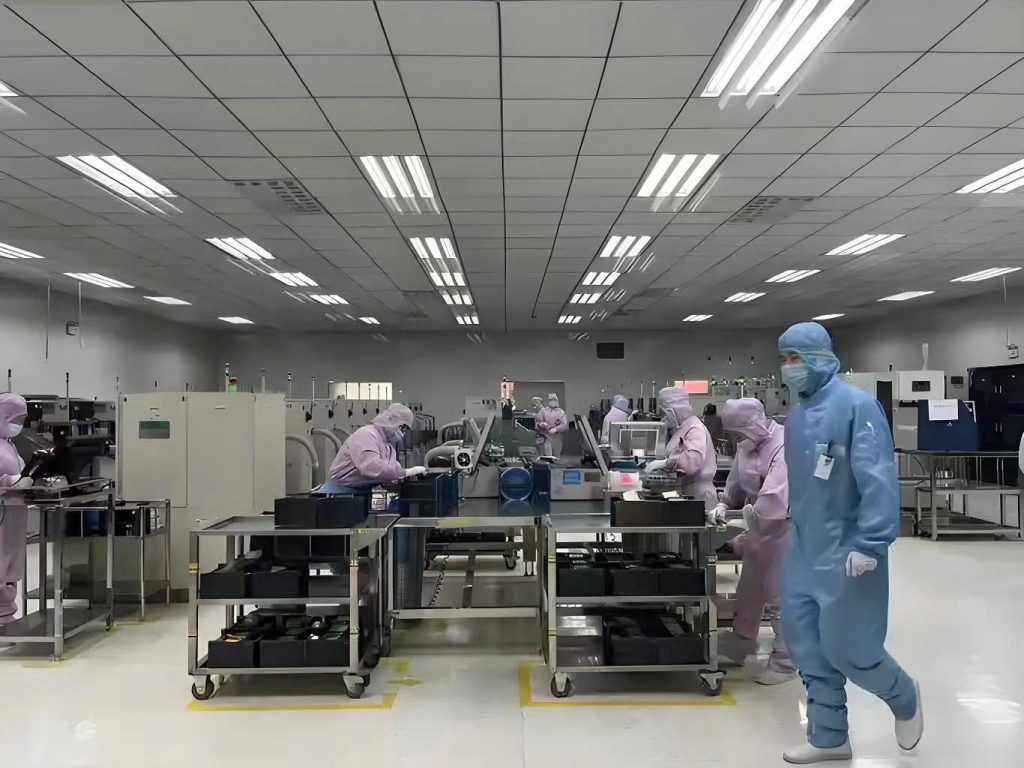
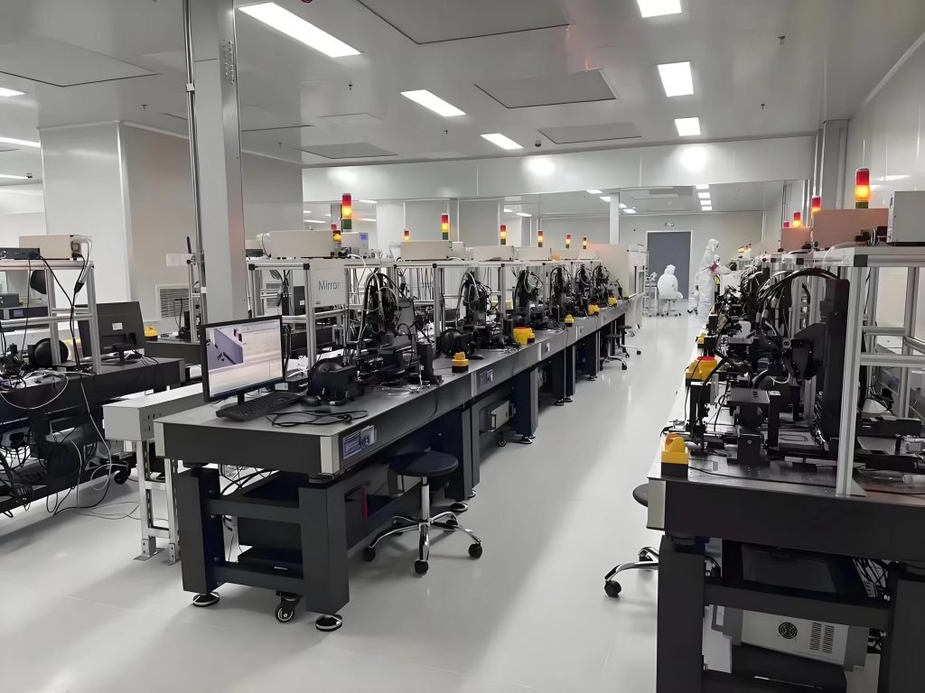
Product album display

Application Areas

  • Industry applications
  1. Solar cells

High photoelectric conversion efficiency: the highest efficiency in the laboratory is 24.2% (2023 data), close to monocrystalline silicon (26.7%), and the theoretical limit is higher (~30%).

Broad spectral response: band gap 1.45 EV, covering visible to near infrared bands, suitable for weak light environment.

Low cost manufacturing: the film thickness is only a few microns, the material consumption is less, and the energy consumption is lower than that of crystalline silicon cells.

Flexible and lightweight: can be deposited on plastic or metal foil, suitable for wearable devices and building integrated photovoltaic (BIPV).

  1. Large photovoltaic power stations

With low cost and high stability, it is suitable for the construction of desert power stations. In 2023, the global production of cadmium telluride components exceeded 11GW, with an annual growth rate of more than 10%.

  1. Special device manufacturing

It is used in infrared detectors, X-ray sensors and light-emitting devices, because its wide band gap (1.45 EV) characteristics are suitable for a variety of photoelectric conversion scenarios

  1. Infrared detector

High sensitivity: excellent response to medium and long wave infrared (3-14 ΜM), suitable for night vision, security and thermal imaging.

Fast response time: up to nanosecond level, better than traditional materials (such as HGCDTE).

No refrigeration: it can work at room temperature, reducing system complexity and cost.


IDM Customization Service

From advanced processes to specialty processes, we use our IDM vertical integration experience to help customers overcome design-process collaboration challenges.

01

Supports advanced nodes such as [5-22nm FinFET/BCD/GAA] to meet the needs of high-performance computing (HPC), AI chips, etc.

02

MPW (Multi-Project Wafer) Service: Small batch trial production to reduce customers' initial costs. Customized process development: Cooperate with customers to conduct DTCO (Design-Process Co-Optimization), customize design rules and process parameters.

03

We support the joint solution of "wafer foundry + advanced packaging" (such as 3D IC, heterogeneous integration) to avoid the loss of multi-supplier collaboration. Unlike pure foundries, we verify the process stability through mass production of our own chips to reduce the risk of tape-out for you.

Provide customers with complete integrated manufacturing services from concept to finished product

01

Electronic manufacturing services and printed circuit board assembly.

02

EMS provides a wide range of electronic manufacturing services, including everything from circuit board design to supply chain management to assembly, testing and after-sales support.

03

PCBA is a link in EMS that focuses on the assembly of printed circuit boards, covering component placement, soldering and related testing, connecting electronic components to manufactured printed circuit boards.

News Center