

Aluminium Arsenide (AiAs)

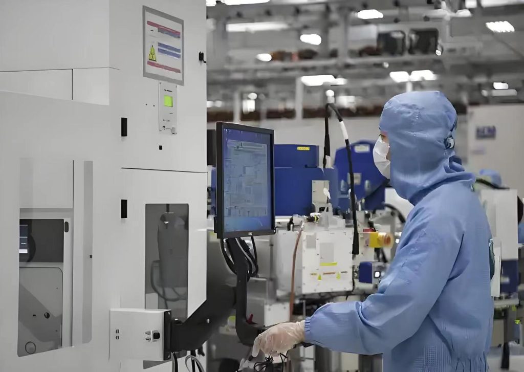
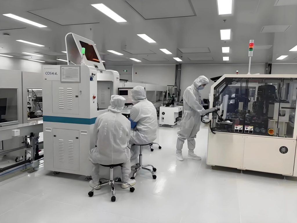
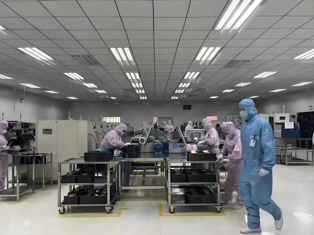
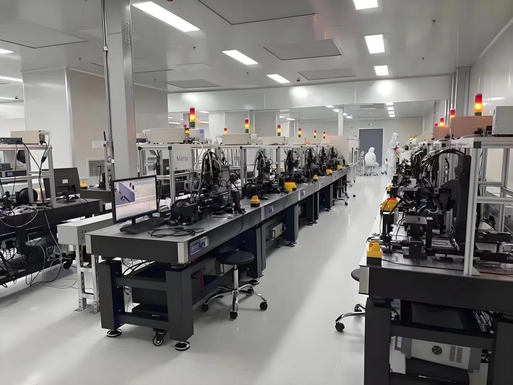
Product album display

Application Areas

  • Industrial application of aluminum arsenide materials
  1. High temperature electronic devices

High temperature resistance: the working temperature can reach more than 500℃, far exceeding silicon (<150℃) and GAAS (<300℃), suitable for aerospace, oil exploration and other extreme environments.

High breakdown field: about 4 x 10⁶ V/CM, suitable for high voltage power electronic devices (such as thyristor, IGBT).

High thermal conductivity: ~0.5 W/CM·K, better than GAAS (0.46 W/CM·K), high heat dissipation efficiency.

  1. Photoelectric devices

Ultraviolet detector: sensitive to 200-400 NM ultraviolet light, fast response (sub-nanosecond), used for flame monitoring, ozone detection.

Laser diode: efficient light emission in the near-infrared band (850-900 NM) combined with GAAS to make vertical cavity surface emitting laser (VCSEL).

Solar cell window layer: as a anti-reflective layer to improve the efficiency of GAAS based laminated cells.

  1. Semiconductor heterostructure

Lattice matching: with a mismatch rate of only 0.12% with GAAS, high quality heterojunctions (such as ALAS/GAAS) can be formed for high frequency transistors (HEMT, HBT).

Electronic limit layer: The high band gap ALAS layer can effectively limit the carrier and improve the device gain and frequency response.

  1. Sensors and MEMS

Pressure sensor: high elastic modulus (~250 GPA) and low thermal expansion coefficient (5.2 x 10-⁶/℃), suitable for high precision pressure measurement.

Microelectromechanical systems (MEMS): used as high temperature resistant structural materials for automotive engine sensors


IDM Customization Service

From advanced processes to specialty processes, we use our IDM vertical integration experience to help customers overcome design-process collaboration challenges.

01

Supports advanced nodes such as [5-22nm FinFET/BCD/GAA] to meet the needs of high-performance computing (HPC), AI chips, etc.

02

MPW (Multi-Project Wafer) Service: Small batch trial production to reduce customers' initial costs. Customized process development: Cooperate with customers to conduct DTCO (Design-Process Co-Optimization), customize design rules and process parameters.

03

We support the joint solution of "wafer foundry + advanced packaging" (such as 3D IC, heterogeneous integration) to avoid the loss of multi-supplier collaboration. Unlike pure foundries, we verify the process stability through mass production of our own chips to reduce the risk of tape-out for you.

Provide customers with complete integrated manufacturing services from concept to finished product

01

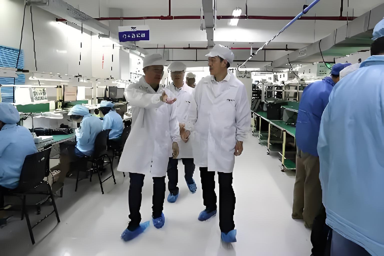
Electronic manufacturing services and printed circuit board assembly.

02

EMS provides a wide range of electronic manufacturing services, including everything from circuit board design to supply chain management to assembly, testing and after-sales support.

03

PCBA is a link in EMS that focuses on the assembly of printed circuit boards, covering component placement, soldering and related testing, connecting electronic components to manufactured printed circuit boards.

News Center