

Gallium Arsenide (GaAs)

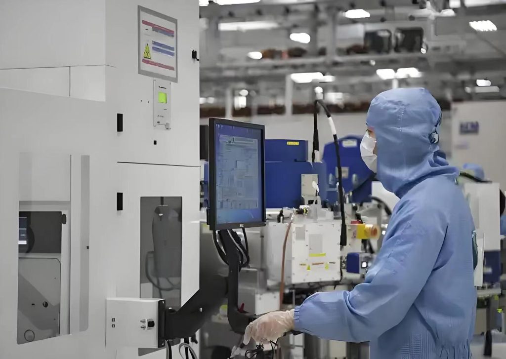
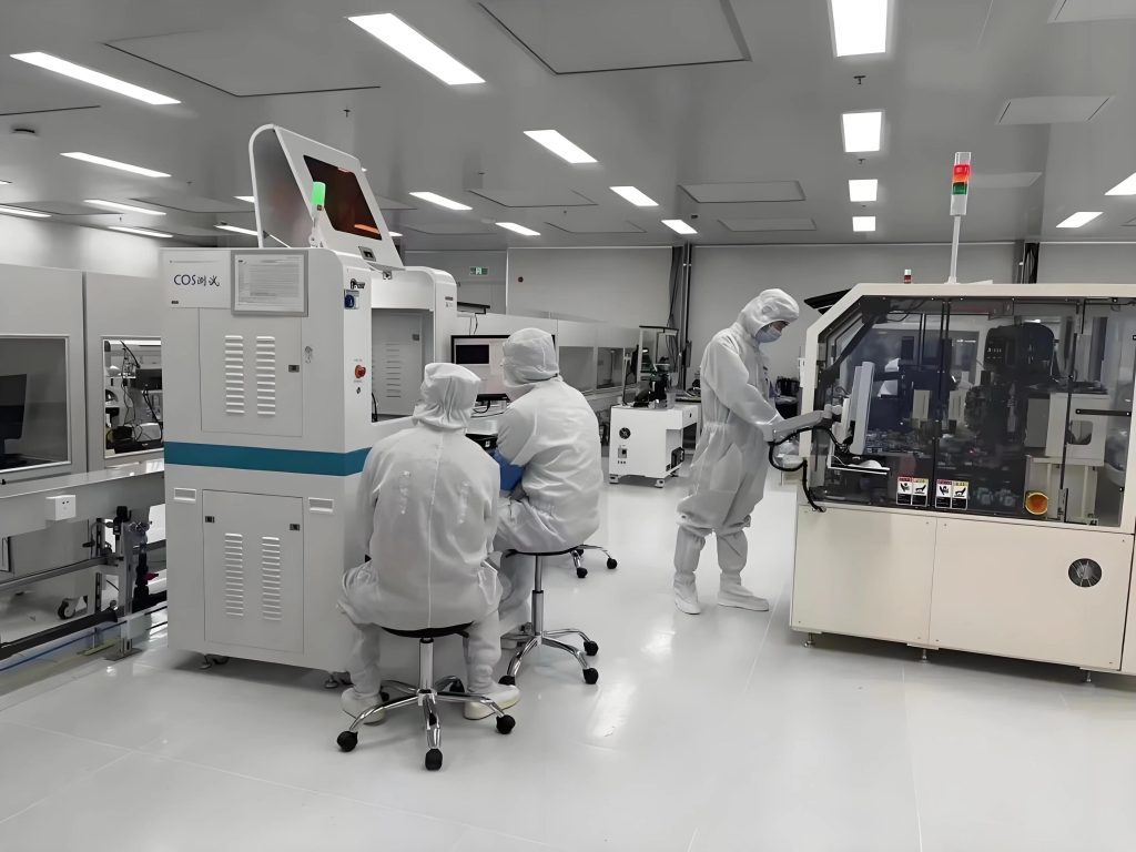
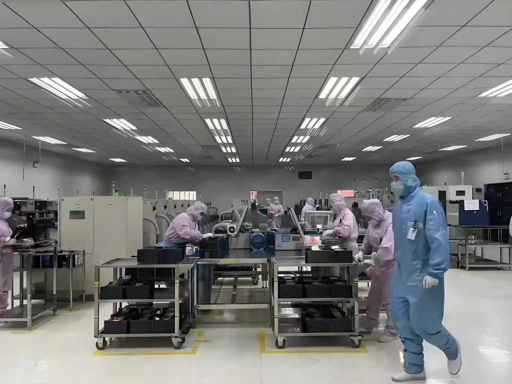
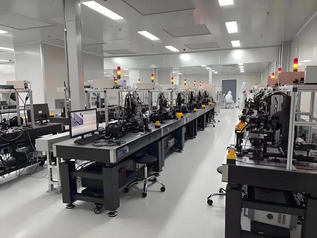
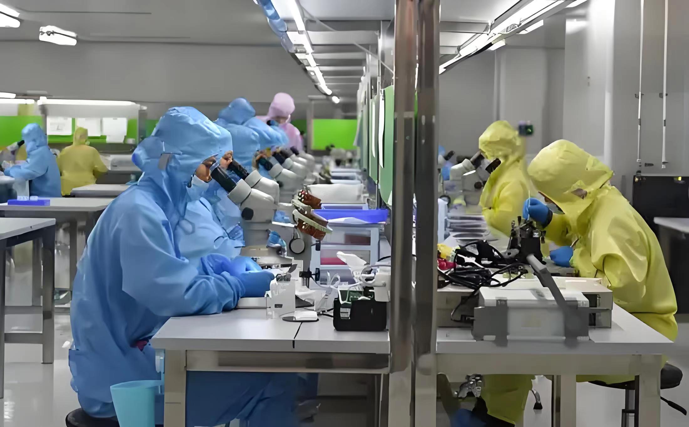
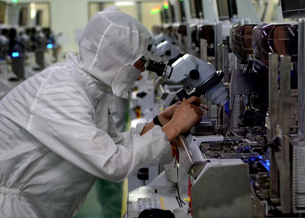
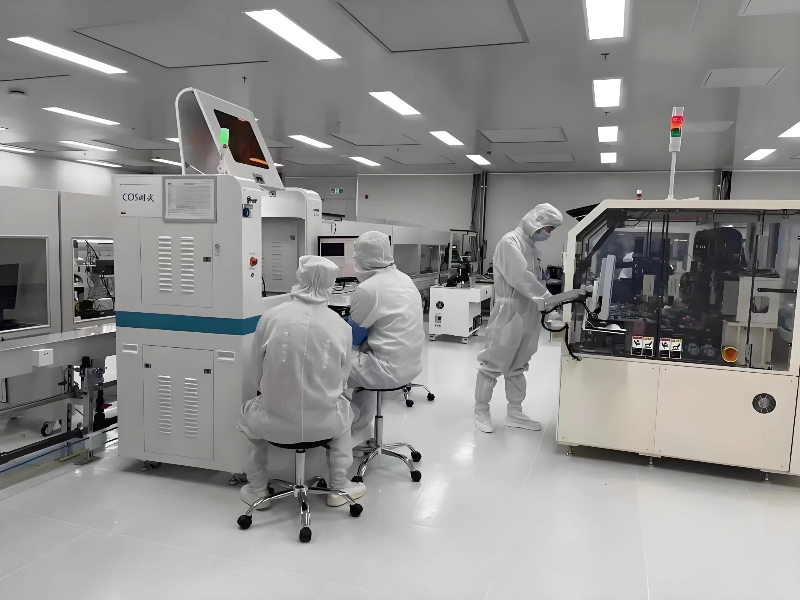
Product album display

Application Areas

  • Advantages of application technical indicators
  1. Technical performance

Through ion implantation or diffusion technology, silicon (SI), zinc (ZN) and other elements are incorporated to adjust the electrical properties of gallium arsenide, and transistors, lasers, solar cells and other devices are manufactured using lithography, etching, deposition and other processes,

High electron mobility: The electron mobility is 8500 CM²/ (V·S), which is 5-6 times that of silicon (much higher than silicon’s 1400CM²/V·S). It is suitable for high frequency and high speed components (5G chips, radar). The breakdown electric field strength is 4×10⁵V/CM, which is suitable for high power RF devices.

Direct band gap structure: The direct band gap characteristic makes its light emission wavelength accurate (near infrared 900NM). It is used for remote control and optical communication module. The conduction band and valence band transition does not need phonon assistance, and the light emission efficiency is high, supporting laser, LED and other optoelectronic devices and detectors.

Negative resistance effect: the current decreases with the increase of voltage under high electric field, which is used in microwave oscillation devices.

High-speed digital circuits: Gallium arsenide resistivity (10⁷-10⁹ Ω·CM) significantly reduces microwave transmission for use in ultra-high speed computers and signal processing systems

Photoelectric conversion rate: Gallium arsenide single-junction solar cells can achieve a conversion efficiency of 28%, and multi-junction cells can achieve an efficiency of more than 40% (silicon cells are about 22%), which is widely used in satellites and spacecraft

High frequency and low noise: Field-effect transistors (MESFET) and high electron mobility transistors (HEMT) can operate at frequencies up to 60GHZ with a noise factor of less than 1DB, suitable for low noise amplifiers (LNA).

Environmental adaptability: heat resistance and radiation resistance: thermal conductivity is 55W/M·K, higher than silicon’s 150W/M·K, suitable for high temperature working environment, strong resistance to high energy particle irradiation, suitable for aerospace and military environment.

Semiconductor insulation: the substrate is electrically isolated by ion implantation to reduce device interference and improve integration.


IDM Customization Service

From advanced processes to specialty processes, we use our IDM vertical integration experience to help customers overcome design-process collaboration challenges.

01

Supports advanced nodes such as [5-22nm FinFET/BCD/GAA] to meet the needs of high-performance computing (HPC), AI chips, etc.

02

MPW (Multi-Project Wafer) Service: Small batch trial production to reduce customers' initial costs. Customized process development: Cooperate with customers to conduct DTCO (Design-Process Co-Optimization), customize design rules and process parameters.

03

We support the joint solution of "wafer foundry + advanced packaging" (such as 3D IC, heterogeneous integration) to avoid the loss of multi-supplier collaboration. Unlike pure foundries, we verify the process stability through mass production of our own chips to reduce the risk of tape-out for you.

Provide customers with complete integrated manufacturing services from concept to finished product

01

Electronic manufacturing services and printed circuit board assembly.

02

EMS provides a wide range of electronic manufacturing services, including everything from circuit board design to supply chain management to assembly, testing and after-sales support.

03

PCBA is a link in EMS that focuses on the assembly of printed circuit boards, covering component placement, soldering and related testing, connecting electronic components to manufactured printed circuit boards.

News Center