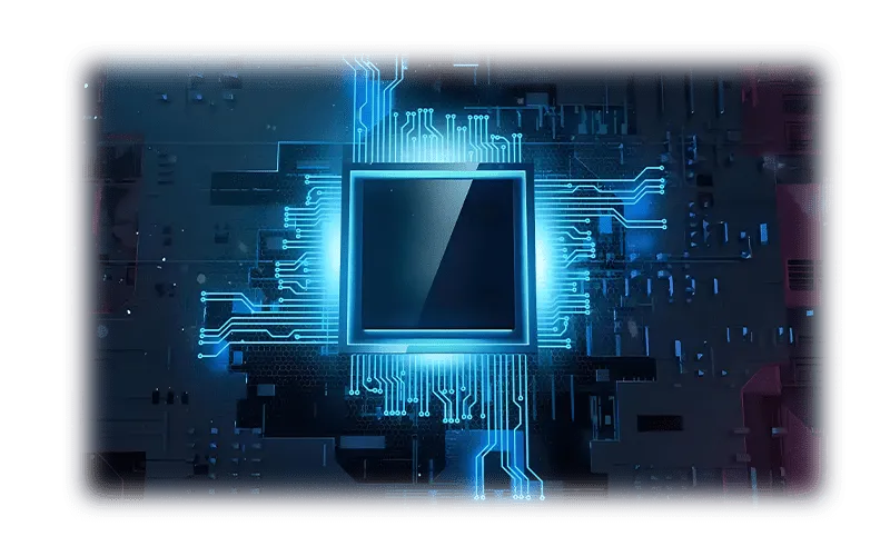
In the age of cloud platforms, AI engines, and streaming services, the pressure on optical networks keeps rising. The choice of semiconductor material has become more than a lab decision—it sets the pace for how your systems perform under real-world stress. Every chip, detector, and transceiver is shaped by the base material that makes it possible. You can’t expect stable links or fast transfers if the material falls short under heat, radiation, or high-frequency demands. That is why companies now look for suppliers who not only ship wafers but also provide a deeper pipeline of services. DEEPETCH, for example, is more than a supplier. With its IDM model, the company runs the full chain from design to finished device, covering both mainstream and specialty semiconductors. They also keep a wide range of chips in stock, which means you are not left waiting when projects need parts quickly. Their story is less about slogans and more about long-term reliability, a trait valued by aerospace, telecom, and next-gen data center clients.

In optical systems, light is the signal carrier. The way semiconductors handle that light determines efficiency, speed, and durability. A poor match between material and wavelength introduces loss. Too much heat and the system drifts. So, the first layer of stability lies in what material is used.
Semiconductors shape how photons are absorbed, transmitted, or converted. This is not abstract theory; it is the foundation for lasers, detectors, and amplifiers in optical networks.
Mobility of electrons, bandgap alignment, and radiation resistance directly affect how quickly data moves. The wrong choice slows the whole system.
Durability comes from thermal behavior and structural strength. In satellites or submarine cables, the wrong material could mean early failure.
Gallium arsenide has been a trusted base for decades. In many ways, it was the first workhorse for optoelectronics. Yet its role today is more specialized, and knowing where it fits helps you plan better.
Gallium Arsenide (GaAs) is known for high electron mobility, allowing faster switching than plain silicon. This makes it suitable for microwave and millimeter-wave circuits that sit beside optical components.

GaAs pairs well with near-infrared light but does not align perfectly with the 1550 nm band, the sweet spot for fiber. That is why it often plays a supporting role, for example in short-distance links or in circuits that condition signals before they hit the long-haul channel.
From amplifiers to testing boards, GaAs wafers provided by DEEPETCH go into systems where speed matters but extreme distance is not the primary concern.
Silicon alone has its limits in optical networks, but adding germanium changes the game. The mix enables detectors and integrated circuits that bridge photonics with electronics.
Silicon And Germanium (SiGe) combines well with established CMOS processes. This allows smoother integration of optical receivers with existing chip lines.
SiGe extends sensitivity into ranges that plain silicon cannot cover. In practice, this makes it a fit for sensing and certain specialty links.
In data centers, SiGe-based detectors can be used in transceiver modules to keep costs manageable while still pushing performance.
Among all three, indium phosphide holds the most critical spot in long-haul and high-speed fiber. It is not by accident—it fits the physics of the job.
Indium Phosphide (InP) has a direct bandgap that aligns with the 1550 nm communication window. This makes it perfect for lasers and detectors in backbone networks.
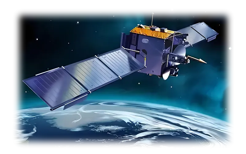
With conductivity around 68 W/m·K and strong resistance to radiation, InP keeps devices stable under load and in harsh environments like space.
In large telecom nodes and hyperscale data centers, InP modules support 400G, 800G, and even 1.6T transceivers. That is why many new deployments are anchored on this material.
Choosing between them is not about which is “best” in every sense. It is about the match between task and material. Each comes with strengths and trade-offs.
GaAs is fast in switching, SiGe is efficient in integration, and InP is unrivaled at high optical bandwidth.
GaAs and SiGe are stable in many uses, but InP shines in radiation-heavy or extreme-temperature cases like satellites.
SiGe is cost-friendly due to CMOS compatibility. GaAs is more niche now, while InP carries higher cost but delivers unmatched performance for top-tier links.
Suppliers vary, but a strong partner covers not just wafers but also downstream needs. This is where integrated models matter.
With IDM operations, DEEPETCH controls design, fabrication, and delivery. Keeping chips in stock reduces lead times for urgent builds.
Clients in defense, telecom, or aerospace can request tailored specs, from wafer thickness to packaging style.
International certifications and years of cross-sector supply have made their materials part of critical systems worldwide.
The demand curve for speed and reliability does not flatten. That means semiconductor materials will keep evolving.
800G and 1.6T are today’s numbers, but multi-terabit networks are already on the horizon. Materials must scale to match.
Future devices may combine GaAs, SiGe, and InP layers to get the best of all worlds in a single package.
Next-gen communication may involve quantum encryption or ultra-fast AI interconnects, where semiconductors must handle single photons or terahertz signals.
Q1: Which material is most widely used in current optical networks?
A: Indium phosphide leads in backbone and high-speed systems due to its alignment with 1550 nm.
Q2: Can GaAs still compete with InP in high-bandwidth systems?
A: GaAs is still strong in microwave and supporting roles but less common for long-distance high-bandwidth links.
Q3: Why is SiGe relevant if InP dominates telecom?
A: SiGe offers cost savings and easy CMOS integration, making it useful for detectors and short-reach links.

The DE-CW-1310 DFB EPI wafer, a high-performance epitaxial structure designed for distributed feedback (DFB) lasers operating at 1310 nm....

Ceramic thin-filmvacuum sensor Optical gas massflowmeter Liquid mass flowmeter Force sensor MEMS...

Photoelectric sensing chip Light source chips Optical transmission and modulationchips Optical detection and receptionchips...

Using a“Detach Core”which has two-layers carrier foil structure on the surface as a core, and forming...

Tenting process is a kind of subtractive process, the process as follows: Laminating photosensitive film...

Modified Semi-Added Process abbreviated as mSAP, which can be used on the core or build-up layers, pattern...

Semi-Added Process abbreviated as SAP, using on the build-up-layer pattern forming as follow:First depositing...

The product generally adopts the pressing lamination process of semi-curing sheets , and line formation...

The products generally adopt the Build-up Film Lamination process, and the circuit formation uses the...

Equipment features: 1. Non-destructive precision testing Micrometer-level probe contact technology...