Chips power everything you touch, from your phone to your car’s dashboard. They’ve changed how industries work, but staying on top means knowing where they came from, what’s holding them back, and what’s next. If you’re hunting for materials or designing new gadgets, this article breaks down the chip world’s journey. A company making waves here, DEEPETCH, kicked off in Shenzhen in 2019. They focus on pure materials, third-generation semiconductors, and everything from wafer production to packaging and testing. Serving consumer tech, automotive, and industrial fields, their team of over 30 (aiming for 50 by 2025) delivers reliable analog ICs and sensors, backed by ISO9001 standards. Their global setup and custom solutions help you tackle the chip industry’s twists and turns.
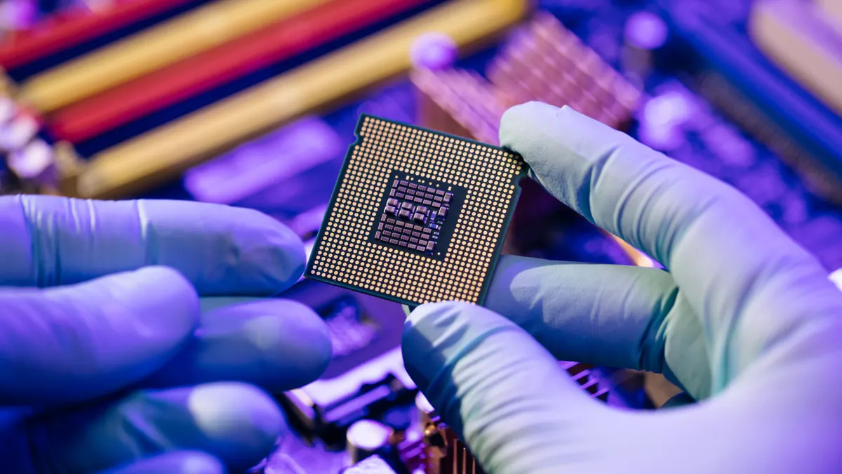
Chips have a wild history. They went from clunky lab experiments to the heart of your devices. A few big moments got them there.
In 1947, the transistor showed up. It ditched bulky vacuum tubes, making electronics tiny. Then, in 1958, Jack Kilby and Robert Noyce built the integrated circuit. They crammed multiple transistors onto one chip. That’s why your phone fits in your pocket today.

Gordon Moore in 1965 said transistor counts would double every couple of years. That guess, called Moore’s Law, pushed tech to zoom forward. Silicon, with a 1.12 eV bandgap and a 1414°C melting point, became the king of materials. It’s tough, forms a handy SiO₂ layer, and keeps your chips solid for mass production.
By the 1990s, the Fabless+Foundry model split design and manufacturing. Bigger 12-inch wafers saved money. Now, IDM solutions mix both steps, building custom chips for your car or IoT gear. It’s like baking a cake at home instead of grabbing one from the store. You get exactly what you want.
Silicon is the chip world’s best buddy. Its special features make it a no-brainer for your projects.
Silicon’s 1.12 eV bandgap hits the sweet spot. It keeps leaks low and switches fast, great for digital circuits. With a 1414°C melting point, it handles the heat of CMOS processes. Your chips stay strong, even in toasty car systems.
Silicon’s everywhere, making up 28% of Earth’s crust. Purified to 99.9999999% with methods like Czochralski, it’s cheap to make. You get wallets-friendly wafers for sensors or processors without spending a fortune.
Silicon grows a natural SiO₂ layer, cutting defects to under 1E10/cm²·eV. That makes MOSFET production a breeze. Its 1500 cm²/(V·s) electron mobility powers 99% of CMOS transistors. Your designs work smoothly with trusted EDA tools and IP libraries.
New materials are shaking things up. You can use them to build chips for special jobs.
Gallium arsenide (GaAs) moves electrons crazy fast at 8500 cm²/(V·s), blowing silicon out of the water. Its direct bandgap makes bright LEDs and laser diodes for fiber optics. You’ll see GaAs in RF amplifiers and satellite systems, giving quick, quiet performance.
Silicon carbide (SiC) nails 23-26% efficiency in solar cells, perfect for electric cars. Gallium nitride (GaN) rocks high-power RF amplifiers with its strong breakdown field. These give you sturdy, power-saving chips for tough tasks.

Diamond’s awesome heat conductivity and carrier mobility make it a future champ for high-power chips. Gallium oxide, with a 4.9 eV bandgap, is another hot pick. You can try these for next-level 5G or aerospace gear. Imagine chips that don’t sweat under pressure!
The chip game has its share of headaches. These issues can mess with your supply chain or project plans.
Squeezing transistors below 2nm brings leaks and overheating. EUV lithography is super accurate but costs millions per wafer. You need smart designs to keep chips fast without emptying your wallet.
Rare materials like gallium, only 0.0019% of Earth’s crust, are tough to find. China supplies 60% of gallium. The Russia-Ukraine conflict jacked copper prices to $10,845/ton in 2022. Those shortages sting. You need dependable suppliers to keep things moving.
Advanced nodes are pricey, a problem for smaller businesses. Chiplet standards like UCIe aren’t ready yet, pushing open markets to the 2030s. Without shared packaging and testing rules, you hit compatibility snags.
A one-stop approach makes these problems easier to handle. It simplifies your chip-building process.
Blending design and manufacturing saves you time. With know-how in wafer production and packaging, this company creates chips from scratch to finish. You get parts that match your needs perfectly. No stress, just results.
This method shines in analog/mixed-signal ICs and sensors. It fits your consumer gadgets and car projects. From pressure sensors (0-3000 bar) to NTC temperature sensors, you get parts that handle rough conditions.
Working with over 50 clients across four industries, a global network keeps materials coming. Mentorship and project swaps mean chips built just for you. This setup lets you sidestep supply chain hiccups with confidence.
The chip world’s moving quick. Here’s what you need to watch to stay in the game.
Chiplets let you mix parts like puzzle pieces, saving cash and adding options. UCIe standards set up an open market by the 2030s. With packaging like FCBGA and SiP, you can make dense AI and HPC chips.
Sensors mixing temperature, humidity, and gas detection power up IoT and self-driving cars. Edge AI handles data right away, boosting your smart home or vehicle systems with tiny, efficient chips.
Low-power designs and recycling cut down on harm to the planet. High-capacity PECVD equipment makes solar cells cheaper and better. You can hit green tech targets without spending too much.
Your projects need a partner you can count on. Since 2019, a Shenzhen-based leader has offered full IDM services, from pure silicon to GaAs and SiC chips. With a team growing past 50 by 2025 and certifications like IATF 16949, you get reliable chips in stock for cars, factories, and gadgets. Their global reach and focus on custom work help you dodge supply risks and build faster. Reach out today to talk chip solutions and lead in a $88.66 billion market by 2029. Picking the right supplier is like finding a great mechanic—you know the job’s done right.
Q1: Why’s silicon the top pick for chips?
A: Silicon’s 1.12 eV bandgap gives solid performance and efficiency. It’s super common, 28% of Earth’s crust, and its SiO₂ layer makes CMOS processes easy and cheap.
Q2: Why are GaAs and SiC big for future chips?
A: GaAs moves electrons fast for RF and LEDs. SiC’s 23-26% efficiency is great for EV chargers. They give you high-performance parts for tough jobs.
Q3: How do supply chain problems hit chip production?
A: Rare materials like gallium are scarce. Conflicts like Russia-Ukraine bump up costs. A diverse supply chain keeps your projects on track.
Q4: How’s sustainability part of chip making?
A: Low-power designs and recycling help the planet. PECVD equipment boosts solar cell efficiency, letting you meet green goals on a budget.

The DE-CW-1310 DFB EPI wafer, a high-performance epitaxial structure designed for distributed feedback (DFB) lasers operating at 1310 nm....

Ceramic thin-filmvacuum sensor Optical gas massflowmeter Liquid mass flowmeter Force sensor MEMS...

Photoelectric sensing chip Light source chips Optical transmission and modulationchips Optical detection and receptionchips...

Using a“Detach Core”which has two-layers carrier foil structure on the surface as a core, and forming...

Tenting process is a kind of subtractive process, the process as follows: Laminating photosensitive film...

Modified Semi-Added Process abbreviated as mSAP, which can be used on the core or build-up layers, pattern...

Semi-Added Process abbreviated as SAP, using on the build-up-layer pattern forming as follow:First depositing...

The product generally adopts the pressing lamination process of semi-curing sheets , and line formation...

The products generally adopt the Build-up Film Lamination process, and the circuit formation uses the...

Equipment features: 1. Non-destructive precision testing Micrometer-level probe contact technology...