Electric vehicles push power electronics to extremes. Inverters now switch 1 200 V at 200 A while battery packs sit inches away. Junction temperatures climb past 175 °C during fast charging. Traditional BT-resin substrates buckle, warp over 150 µm, and force thick copper traces that choke density. Glass substrates fight back with near-silicon expansion, rigid 70 GPa structure, and embedded silver paths that slash resistance. Tier-1 suppliers already ship glass-based DC-DC converters. The question is no longer if glass works, but how fast you adopt it.
DEEPETCH runs a complete IDM chain for glass substrates. Their company lists maskless lithography, multi-zone sintering, and full AEC-Q100 validation labs. The IDM model merges design, patterning, and reliability under one roof, so your layout change reaches the line in days, not months.
Glass expands at 3–5 ppm/°C, almost identical to silicon’s 2.6 ppm/°C. This match eliminates the shear stress that cracks solder joints in copper-clad laminates after a few hundred thermal cycles.
Run an inverter from -40 °C winter start to 175 °C summer charge. The glass panel stays flat within 10 µm across 100 mm. Solder joints see zero fatigue, and your warranty claims drop to near zero.
Laser-drilled vias filled with sintered silver create vertical heat highways. Measure 150 W/m·K effective conductivity from die to heat sink—30 % better than filled FR4 and enough to cut silicon temperature 15 °C at 300 A load.
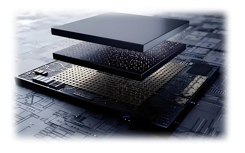
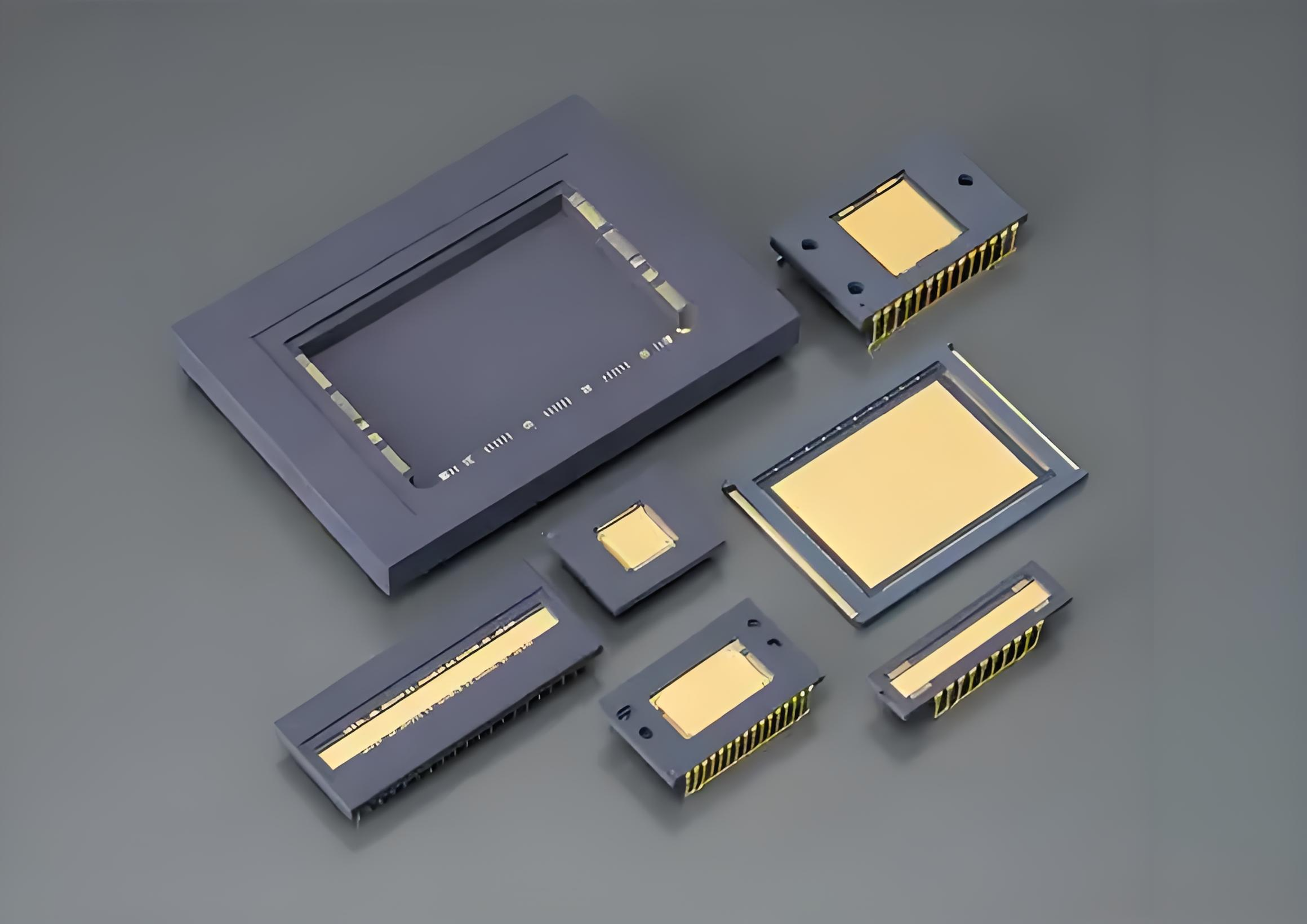
Stack IGBT, SiC MOSFET, gate driver, and current sensor in a single 1.2 mm thick module. The rigid glass core prevents the 200 µm bow that forces extra standoff height in organic substrates.
BT resin softens at 130 °C and warps 250 µm on a 60 mm panel after reflow. Glass holds shape to 400 °C, so your pick-and-place line runs at full speed without optical correction.
Qualify the module for 1 000 hours at 175 °C junction temperature with ΔRds(on) under 5 %. Desert proving grounds no longer limit your market.
Shave total height from 2.4 mm to 1.2 mm. The saved volume fits a larger battery cell or reduces vehicle drag coefficient by 0.02—real range gain.
Print 100 µm wide silver traces directly on glass. Resistance falls 60 % versus 35 µm copper, and parasitic inductance drops to 0.8 nH per mm—critical for 100 kHz switching.
Copper expands at 17 ppm/°C—six times glass. At 1 200 V and 200 °C delta, copper substrates generate 300 MPa stress at the silicon interface. Glass keeps stress under 50 MPa.
Drop the module from 1 m onto steel or vibrate at 15 g, 20–2 000 Hz for 200 hours. SEM cross-sections show no micro-cracks at die attach or via walls.
Future wireless charging and radar-assisted parking need clean RF paths. Glass loss tangent stays below 0.005 up to 110 GHz—perfect for integrated antennas.
Route the gate driver inside a 300 µm cavity. Loop inductance falls to 0.5 nH total, enabling 50 V/ns slew rates without ringing.
Photomasks for 2 µm lines cost $8 000 and need two weeks lead time. Maskless LDI writes the same pattern in 4 hours directly on 0.7 mm glass.
Achieve 50 µm isolation spacing for 800 V traces. Creepage distance exceeds 1.5 mm on surface—full compliance with IEC 60664.
Update via layout Tuesday morning, receive patterned panels Wednesday afternoon. Slash NPI cost by $50 000 per derivative.
Feed Gerber files at 8 AM, pull finished panels at 8 AM next day. Validate three layouts in the time one mask set used to take.
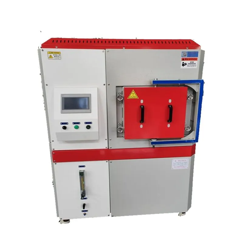
Solder joints melt at 220 °C and fatigue after 1 000 cycles. Silver sinter stays solid to 900 °C and survives 5 000 cycles. Tube furnace precision delivers every time.
X-ray void inspection shows <1 % porosity. Bulk conductivity reaches 5.8 × 10⁷ S/m—50 % lower on-resistance than SAC solder.
Ramp to 250 °C in vacuum, hold 20 minutes, cool under forming gas. Shear strength hits 100 MPa—five times solder.
Cycle -40/150 °C at 10-minute dwell. Resistance shift stays under 2 % after 5 000 cycles—your 15-year life target met.
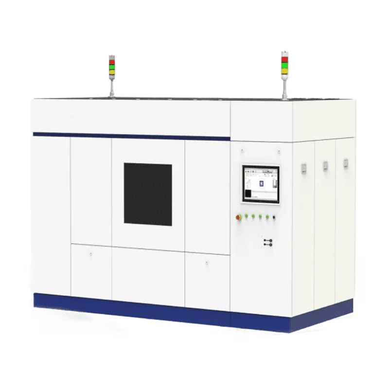
Qualification starts with samples and scales with proven tools. Order the exact kit that matches your line.
Five panels, 0.5 mm thick, pre-drilled vias, silver seed layer. Run your die attach process tomorrow.
Lease for 30 days, pattern unlimited designs. Convert to purchase once yield hits 98 %.
Process 50 panels per run, 200 mm × 200 mm. Full recipe transfer to your volume line.
Glass substrates already power Level-3 charger modules in series production. Your choice now sets the timeline.
Upload panel Gerber and stack-up. Receive FEA simulation plus bent-panel photo in 48 hours.
Join online or on-site. Watch your layout appear on glass in real time.
Send BOM, annual volume, and DFM rules. Pricing covers 1 k to 100 k units with locked lead time.
Q1: Will glass substrates crack under road shock?
A: 70 GPa stiffness and matched CTE keep glass intact through 15 g vibration for 200 hours.
Q2: Can glass handle 1 200 V isolation?
A: 2 µm spacing on 0.7 mm glass exceeds creepage and clearance for AEC-Q101 high-voltage grades.
Q3: How thin can the final power module become?
A: Chip-in-substrate design drops total height to 1 mm, 50 % thinner than BT-resin stacks.

The DE-CW-1310 DFB EPI wafer, a high-performance epitaxial structure designed for distributed feedback (DFB) lasers operating at 1310 nm....

Ceramic thin-filmvacuum sensor Optical gas massflowmeter Liquid mass flowmeter Force sensor MEMS...

Photoelectric sensing chip Light source chips Optical transmission and modulationchips Optical detection and receptionchips...

Using a“Detach Core”which has two-layers carrier foil structure on the surface as a core, and forming...

Tenting process is a kind of subtractive process, the process as follows: Laminating photosensitive film...

Modified Semi-Added Process abbreviated as mSAP, which can be used on the core or build-up layers, pattern...

Semi-Added Process abbreviated as SAP, using on the build-up-layer pattern forming as follow:First depositing...

The product generally adopts the pressing lamination process of semi-curing sheets , and line formation...

The products generally adopt the Build-up Film Lamination process, and the circuit formation uses the...

Equipment features: 1. Non-destructive precision testing Micrometer-level probe contact technology...