In the complicated world of semiconductor production, a successful output often relies on one simple part: the carrier. As your valuable substrates move through a huge number of detailed processing stages, their safety depends completely on the special trays built to protect them. The entire path, starting from a large, raw wafer—the core substrate—and finishing with thousands of separated, working chips, involves a major change in handling needs. A Wafer Carrier Tray and a Chip Holder (Die Tray) are completely different tools; they are made for two separate parts of making the chip: large-scale process defense versus very tiny, exact handling. Ignoring this basic difference risks material damage, contamination, and profit loss.

Modern compound semiconductors like GaAs, SiC, and GaN push the limits of older carrier designs. These high-tech materials are naturally more demanding than standard Monocrystalline silicon.
Materials like Gallium Arsenide (GaAs) are delicate and break easily during automated movement, which can cause tiny cracks or chipping. Because GaAs substrates are crucial for high-frequency electronics and light-based devices—due to their high electron mobility,—they are very costly. Any damage means a direct financial hit, so a specialized carrier is needed to actively lessen mechanical stress points throughout the process.
Advanced devices are extremely sensitive to pollution. Metal ions coming from the carrier itself can act as harmful impurities, greatly lowering the electronic and optical quality of the final chip. This is why the carrier must be chemically stable, non-shedding, and extremely pure, because it must keep the wafer surface perfect.
For high-value materials, expertise in material science is key. DEEPETCH, an IDM company, oversees the whole process from raw materials to final packaging. This integrated approach means their carrier designs use technical insight into the substrate’s stress tolerance and pollution sensitivity. As a result, they ensure the carrier material is compatible from the moment the raw wafer enters your facility.
The Wafer Carrier Tray works in the early stages of fabrication, facing harsh chemical and thermal environments. Its main job is to defend the single, high-cost wafer through corrosive wet chemical dips, plasma etching, and high-heat thermal treatments. Because this phase involves large-scale handling, the main goal is to keep the entire substrate flat and whole.
Wafers, especially those made thinner than 100 μm for MEMS devices, can easily bend or break if handling errors occur. Frontend carriers must use specialized edge-grip or V-groove support designs, which keep the main device area untouched while giving gentle, stable support across the entire wafer surface.
Robot movement builds up static charges, which can instantly ruin sensitive electronic parts. Therefore, a reliable Wafer Carrier Tray must use materials that safely reduce static electricity. This allows charges to leave the carrier slowly without adding conductive pollutants, protecting sensitive circuitry.
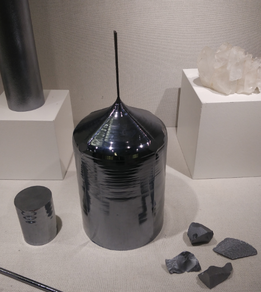
Since compound semiconductors like SiC and GaN require high-power processes, production often involves very high temperatures, sometimes over 1600℃. Standard plastic carriers cannot survive this. You must switch to materials like high-purity Quartz or Isostatically Pressed Graphite, because these offer the necessary thermal stability and chemical resistance to stop structure failures during extreme heat steps.
Once the wafer is cut into individual chips (dicing), the focus shifts from a large circle to small squares. The Chip Holder replaces the Wafer Carrier Tray, demanding exact positioning and easy access for assembly. The focus changes from the whole circular piece to the precise spot of every single square die.
The Wafer Carrier is made for bulk protection of a large circle. The Chip Holder, in contrast, is a tiny positioning grid, built to hold thousands of individual dies in exact spots. This means the manufacturing limits change from general millimeter clearance to micrometer-level exactness.
After dicing, chips are placed into the Chip Holder. This tray acts as the stable reference point for all subsequent automated assembly steps. If the chips are not aligned perfectly within the holder’s pocket, automated machines like wire bonders will fail, leading to immediate yield loss when the chips are most valuable.
The Chip Holder is specifically engineered for final assembly. For advanced packaging like the FCBGA Substrate (Flip-Chip Ball Grid Array), the IC chip is placed inside the substrate. This needs the holder to have a special, flat shape that works with the structure of these packages, supporting the move to lighter and thinner finished parts. This exact positioning is also vital for the Sensor chip series.
The carrier material choice is a core engineering decision based on the harshest conditions it will face. Making the wrong choice will definitely lead to contamination or structural failure.
For cleaning and wet etching that use strong chemicals, you must use high-quality engineering plastics. Materials like PEEK (Polyether Ether Ketone) or PTFE (Polytetrafluoroethylene) resist chemicals very well and outgas little, which prevents pollution of the sensitive solutions.
When temperatures go above 500℃ (e.g., SiC power devices), standard plastics melt. You must use high-purity, thermally stable types like Quartz or specially pressed Graphite.
For very sensitive parts, such as MEMS sensors in the Sensor chip series, static dissipative polymers with specific additives are used. These materials safely stop charge from building up, protecting tiny structures from permanent damage.
In summary, the transition from wafer to chip handling is a complete shift in demands—from bulk protection against harsh environments to micrometer-level precision for assembly. Selecting a carrier is not just about moving material; it’s about perfectly matching the carrier’s material, design, and tolerance to the exact stage and fragility of the semiconductor product, guaranteeing the highest possible yield and performance at every step.
Q1: What is the primary functional difference between a wafer carrier and a chip holder?
A: The Wafer Carrier (Tray/Boat) is made for large-scale protection of the whole, raw wafer during processing steps (like high heat and chemicals), while the Chip Holder (Die Tray) is made for very exact positioning of thousands of small, cut dies during final assembly and testing.
Q2: How does the IDM model improve carrier design accuracy?
A: The IDM model ensures that the carrier design is based on direct, deep knowledge of the raw wafer material’s specific weaknesses, process needs, and pollution risks, so the carrier material and shape are perfectly matched to keep the wafer safe during processing.
Q3: What is the role of the chip holder when dealing with advanced packaging like FCBGA?
A: For advanced packaging, the Chip Holder’s main job is to provide precise positioning for the separated die, which is necessary for automated bonding. It must be designed to work with the final package structure, supporting the move to thinner and lighter finished parts.

The DE-CW-1310 DFB EPI wafer, a high-performance epitaxial structure designed for distributed feedback (DFB) lasers operating at 1310 nm....

Ceramic thin-filmvacuum sensor Optical gas massflowmeter Liquid mass flowmeter Force sensor MEMS...

Photoelectric sensing chip Light source chips Optical transmission and modulationchips Optical detection and receptionchips...

Using a“Detach Core”which has two-layers carrier foil structure on the surface as a core, and forming...

Tenting process is a kind of subtractive process, the process as follows: Laminating photosensitive film...

Modified Semi-Added Process abbreviated as mSAP, which can be used on the core or build-up layers, pattern...

Semi-Added Process abbreviated as SAP, using on the build-up-layer pattern forming as follow:First depositing...

The product generally adopts the pressing lamination process of semi-curing sheets , and line formation...

The products generally adopt the Build-up Film Lamination process, and the circuit formation uses the...

Equipment features: 1. Non-destructive precision testing Micrometer-level probe contact technology...