As the digital world moves into 2026, the rise of artificial intelligence, 6G networks, and large-scale data centers has created huge needs for network bandwidth. Optical modules, which handle electro-optical conversion, are seeing major changes to tackle these issues. These plug-in transceivers are now essential parts of high-performance computing, and they support the quick-response and high-capacity setups needed for the future. If you want a strong way to boost network work, understanding the patterns in advanced optical modules will help you stay ahead in a fast-changing market.
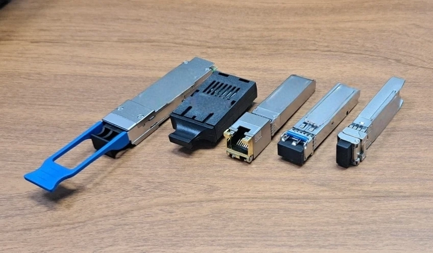
The fast rise in data flow shows that standard communication gear has hit its hardware limits. By 2026, the sector has moved from steady 400G systems to 800G, and 1.6T development is speeding up. This change means optical modules must keep small sizes while offering better integration and less power use to manage more complex computing setups.

To meet big data handling demands, the inside build of optical modules is shifting in basic ways, since early standards no longer fit the needs of current smart computing centers, and this leads to wide use of advanced packaging methods known for tight packing and low energy use. Plug-in designs let you grow and fix your network without stopping service, which provides the flexibility essential in the changing connection world of 2026.
In this tech shift, DEEPETCH shines with its strong research and development skills. Started in 2019, the company aims to supply fresh products for worldwide data centers and supercomputing sites, and it has reached large output of 400G/800G high-speed optical modules. As a top IDM (Integrated Device Manufacturer), their work covers the full industry chain from chip design and wafer making to packaging and checking. Whether you need liquid cooling fixes or custom AOC and DAC cables, their background in helping over 1,500 clients around the world gives the solid tech backing you require.
When you check the next wave of optical transceivers, focus on bit error rate under heavy load. The rules for 2026 demand that modules keep low signal loss even at full capacity, and by adding strong DSP chips and fix algorithms, current optical modules handle spread effects in send paths well, which keeps data solid over long reaches.
The work of an optical module rests mainly on the quality of its inner semiconductor chips, and a top transceiver uses compound semiconductor materials with good carrier movement and broad bandgaps. In the 2026 market, advances in material work directly set the reach and accuracy of optical signal sends, acting as the best way to cut signal delay.
Indium Phosphide (InP) and Gallium Arsenide (GaAs) form the base for high-frequency and high-speed electronic parts. GaAs sees wide use in making LEDs and lasers because of its direct energy gap, while InP serves as the main material for long-distance fiber optic links. By fine-tuning the electronic traits of these bases, you gain better carrier movement and less noise. This setup lets your network hold high conversion work even at very high frequencies.
Standard organic bases often deal with big electrical signal loss in high-frequency spots. Better options in 2026 lean toward glass or ceramic bases. Glass bases work as insulators with very low electrical loss and good heat steadiness. When paired with special laser mask projection methods, the stick of silver layers to the glass face improves a lot. This exact making lets IC chips sit inside the base, so the full optical module package gets smaller, slimmer, and fits well with current build plans.
Thin film deposition methods play a key part in building exact optical parts like lenses and filters. By guiding the deposition at the atom level, you can set light passage and reflection just right. This tiny-scale making not only boosts the sense skill of optical transceivers but also raises material hold against wear and rust, which lengthens the use time of modules in tough industrial spots.
As optical module speeds go up, heat control turns into the main element for network steadiness, since poor heat spread can shorten laser life fast and lead to full link breakdown. Thus, picking packaging with good heat flow and strict test steps is your way to keep business running smooth.

Ceramic packaging stays the best pick for high-work lasers in 2026. Next to usual materials, ceramics give very high heat flow and strong mechanical build, which spreads the strong heat from inner parts well. This matters a lot for communication gear in hard settings. Through set thin-film deposition ways, optical modules keep steady frequency answer over a broad heat range, dodging signal twist from heat shift.
To make sure each optical module sent out hits industry rules, a tough check process is a must. Using X-ray checks and IV curve review helps spot and cut out possible build flaws. In the Chips In-Stock service, this drive for quality means every part you get has high steadiness, which lowers your ongoing fix costs.
Current network spots grow more varied, from wet undersea cable sites to hot industrial auto shops. Optical modules need strong fit to surroundings. Through picked materials and seal methods, advanced optical modules stand up to shakes, hits, and medium wear. This full guard keeps your data stream steady even in the roughest physical spots.
With varied use cases, off-the-shelf products often fail to match cost and work balance. The strength of the IDM model comes from linking design and making closely, which offers deep custom system fixes based on your exact wants.
The IDM model brings special gains in making MEMS and special process semiconductors. By running factories and controlling key steps, a maker can guide atom-level deposition for set function layers in optical transceivers. Whether building exact optical parts or boosting material toughness, this full-step hold cuts the time from research to big output a lot.
Going forward, optical modules will do more than send data. By adding surroundings sensors and edge AI process chips, future transceivers can check network states live. This multi-way mix feels heat and wet while watching small changes in optical power. If you want these new fixes, reach out to tech pros via the Contact Us page to shape a communication plan for your setup.
In a world of shaky global supply lines, steady big output ability is a company’s core strength. By linking production steps top to bottom, top makers shift capacity as needed to meet sudden market jumps. This in-house make from wafer to module makes sure that in the unsure 2026 market, you get a reliable and quality-good supply.
Q1: What are the main advantages of hot-pluggable optical modules?
A: Hot-pluggability lets you swap or update modules right in the network system without shutdown, which boosts fix work and cuts gear stop time.
Q2: Why is the 800G optical module becoming the standard in 2026?
A: As bandwidth needs grow for AI model training, old 400G fails to hit high flow rules, so 800G and above become the usual setup for smart computing centers.
Q3: How does the IDM model benefit my procurement process?
A: The IDM model keeps high match from chip research to end send, offering more bendable custom services, better capacity promises, and tighter quality checks.

The DE-CW-1310 DFB EPI wafer, a high-performance epitaxial structure designed for distributed feedback (DFB) lasers operating at 1310 nm....

Ceramic thin-filmvacuum sensor Optical gas massflowmeter Liquid mass flowmeter Force sensor MEMS...

Photoelectric sensing chip Light source chips Optical transmission and modulationchips Optical detection and receptionchips...

Using a“Detach Core”which has two-layers carrier foil structure on the surface as a core, and forming...

Tenting process is a kind of subtractive process, the process as follows: Laminating photosensitive film...

Modified Semi-Added Process abbreviated as mSAP, which can be used on the core or build-up layers, pattern...

Semi-Added Process abbreviated as SAP, using on the build-up-layer pattern forming as follow:First depositing...

The product generally adopts the pressing lamination process of semi-curing sheets , and line formation...

The products generally adopt the Build-up Film Lamination process, and the circuit formation uses the...

Equipment features: 1. Non-destructive precision testing Micrometer-level probe contact technology...