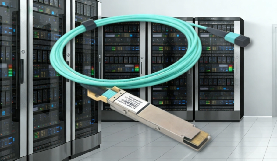
The quick growth of AI computing, 5G networks, and large-scale data centers has driven traditional copper-based data transmission to its physical boundaries. Optical chips now serve as the key element for high-bandwidth communication in modern network designs. Yet, the basic performance of a silicon photonics chip or a laser diode depends heavily on the enclosure that shields it. Packaging connects the sensitive micro-scale world of photons to the strong demands of global telecommunications. Selecting the proper method decides if the system reaches top efficiency or suffers from signal loss and heat-related issues.
Before exploring the specific area of photonics, it is essential to understand the basic packaging technologies that support the wider semiconductor sector. Standard electronic packaging fulfills three main roles: power supply, signal linking, and protection from the environment. In high-performance uses, ceramic materials often outperform plastic due to their better sealing and heat transfer properties.

This traditional format employs a ceramic body to contain the chip. It offers strong defense against moisture and tough conditions. Although it is less used in high-speed data now, it stays a dependable option for industrial sensors and parts that need high durability.
Designs that require more leads without expanding the size much benefit from this square package. It features leads on all four sides. Thus, it suits tight spaces where signal quality must hold across various input/output ports.
These approaches use the package’s bottom for connections, supporting hundreds of pins. Ball Grid Array (BGA) works well for high-speed digital chips. The reason is that the shorter route from chip to board cuts down on unwanted inductance.
Current production lines require packages that fit automated SMT processes. Ceramic packages built for SMT enable dense board arrangements. At the same time, they provide the mechanical robustness needed for lasting reliability in infrastructure.
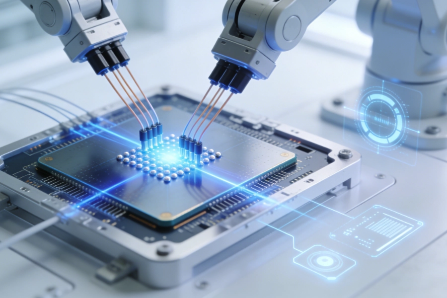
Optical chips vary greatly from electrical ICs since they handle light rather than electrons alone. Challenges include precise micron-scale alignment, exact temperature regulation, and blocking even tiny amounts of water from the light path. For high-speed needs, experts generally favor a targeted approach that handles these issues effectively.
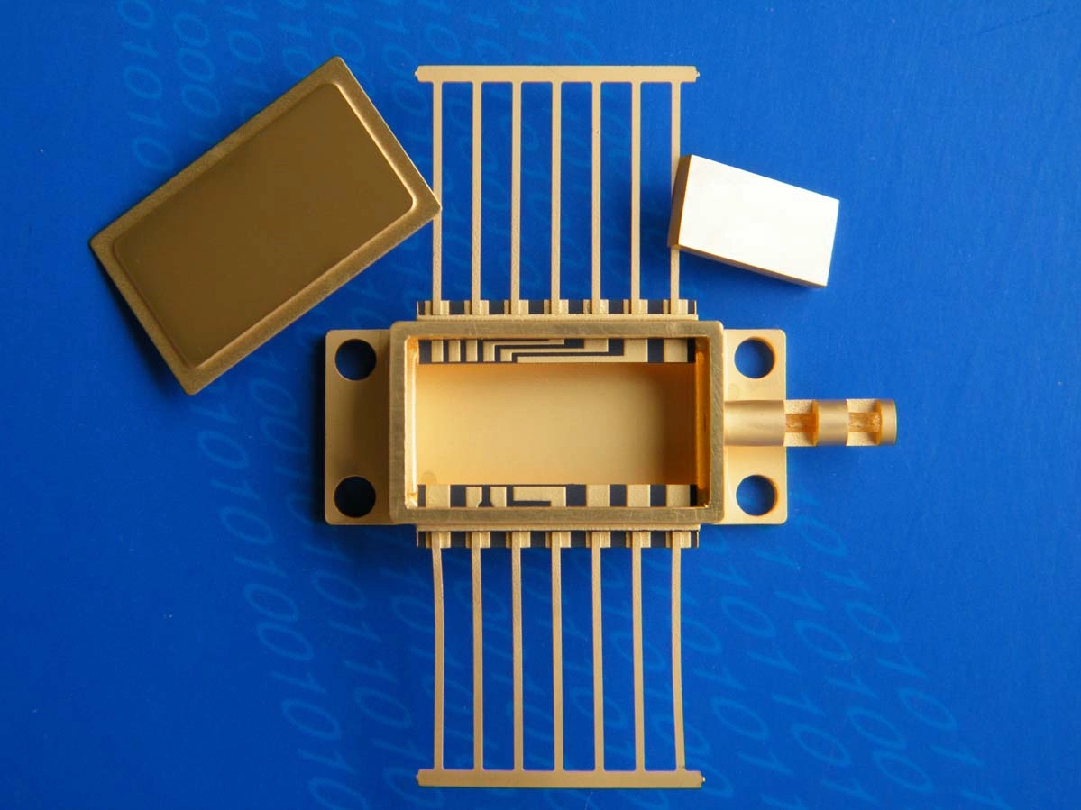
Laser diodes and modulators in the Communications Industry often use the butterfly package as the top choice. Its distinct “butterfly wing” lead setup lets high-frequency electrical signals enter from the sides. Meanwhile, the optical fiber exits from the front, which cuts down on interference.
Optical function depends strongly on temperature; even small heat changes can alter a laser’s wavelength. The Butterfly package offers sufficient space inside to include a TEC and a thermistor. As a result, it allows tight control of the chip’s temperature.
Plastic packages can take in moisture gradually, but ceramic-to-metal seals create a fully airtight space. This stops oxidation of sensitive optical layers. Such protection proves crucial in areas with changing humidity levels.
At speeds like 400G and 800G, the material’s electrical traits matter a lot. High-purity ceramics deliver low signal loss. Therefore, they ensure high-speed data drivers activate the optical chip without much shape distortion in the signals.
Scaling networks to handle AI training clusters reveals clear physical limits. High-speed data communication involves more than just chip speed. It requires managing the physics across the full connection path.
Frequencies for 800G transmission cause signals to stick to conductor surfaces, known as the skin effect. Poor materials absorb these signals easily. Packaging must shorten the path from electrical driver to optical emitter to avoid signal spreading.
High-speed transceivers produce notable local heat. Without proper removal, light conversion efficiency falls, creating more heat and less output. Advanced packaging serves as a main heat remover to keep the system steady.
Optical fiber cores in high-speed links measure just a few microns across. Packaging needs a firm mechanical base that withstands heat expansion. This keeps the fiber aligned with the chip’s active zone for a decade or more.
In this demanding field, a partner with full control over the tech stack is vital. DEEPETCH excels as a top IDM (Integrated Device Manufacturer). They go beyond design by making the chips themselves. Started in 2019, the company has grown fast to serve more than 1,560 clients worldwide in data centers and AI computing. Their combined approach to design, wafer production, and advanced packaging avoids typical gaps in “design-only” setups. For 400G/800G liquid-cooled transceivers or tailored sensor options, this integration optimizes the package for the inner silicon. Their wide Chips in Stock help speed up market entry.
Owning the full production lets them adjust ceramic substrate features to fit exact optical needs. This provides optimization levels that companies without fabs cannot achieve. As a result, the packaging matches the chip’s requirements closely.
Supply chain issues make steady access to high-speed parts a key benefit. DEEPETCH’s strong setup in Shenzhen and Hong Kong keeps production running smoothly. This reliability supports ongoing operations without delays.
Facilities follow strict rules like IATF 16949 and ISO 9001. This focus on quality ensures every package, from basic sensors to complex 800G modules, hits the dependability marks for critical systems. Thus, long-term performance remains secure.
The sector heads toward closer integration for speeds past 1.6T. Standard plug-in modules might fade as new setups bring light nearer to the core processor.
CPO marks the coming wave, where the optical unit joins the switch silicon on one base. This cuts power use by up to 30% by removing long electrical paths to the board edge. Such efficiency boosts overall system performance.
Crowded data centers drive needs for smaller sizes. “Wafer-level packaging” for optics will rise, sealing and checking hundreds of chips at once before cutting. This method speeds production and lowers costs.
800G modules test power boundaries, making air cooling outdated. New designs include liquid-cooling links to draw heat straight from the chip face with special fluids. This keeps operations cool and reliable.
Q1: Why is the butterfly package preferred for lasers?
A: It provides a stable, hermetic environment with built-in temperature control (TEC), which is essential for maintaining the wavelength stability and longevity of laser chips.
Q2: What is the benefit of the IDM model in chip packaging?
A: The IDM model allows for seamless coordination between chip design and package manufacturing, ensuring the housing is perfectly optimized for the chip’s thermal and electrical needs.
Q3: How does ceramic packaging compare to plastic for optical chips?
A: Ceramic offers superior heat dissipation, better high-frequency electrical performance, and a true hermetic seal that prevents moisture from damaging optical components.
Q4: What role does packaging play in 800G data transmission?
A: At 800G, packaging is critical for reducing signal attenuation and managing the intense heat generated by high-speed optoelectronic conversion.
Q5: Is SMT compatibility important for optical modules?
A: Yes, SMT compatibility allows optical components to be mounted using standard high-speed assembly lines, reducing manufacturing costs and improving board-level reliability.

The DE-CW-1310 DFB EPI wafer, a high-performance epitaxial structure designed for distributed feedback (DFB) lasers operating at 1310 nm....

Ceramic thin-filmvacuum sensor Optical gas massflowmeter Liquid mass flowmeter Force sensor MEMS...

Photoelectric sensing chip Light source chips Optical transmission and modulationchips Optical detection and receptionchips...

Using a“Detach Core”which has two-layers carrier foil structure on the surface as a core, and forming...

Tenting process is a kind of subtractive process, the process as follows: Laminating photosensitive film...

Modified Semi-Added Process abbreviated as mSAP, which can be used on the core or build-up layers, pattern...

Semi-Added Process abbreviated as SAP, using on the build-up-layer pattern forming as follow:First depositing...

The product generally adopts the pressing lamination process of semi-curing sheets , and line formation...

The products generally adopt the Build-up Film Lamination process, and the circuit formation uses the...

Equipment features: 1. Non-destructive precision testing Micrometer-level probe contact technology...