In today’s world, where data grows twice as fast every year and a half and huge AI computers need lightning-fast connections, optical chips have quietly become the real heroes of modern communication. These tiny chips create, shape, guide, and catch light right inside themselves. They leave old copper wires far behind because light carries information much faster, with far less heat and power waste. No matter whether you are making the newest 800G internet modules, putting lasers right next to AI chips, or building self-driving car sensors, everything starts with a good optical chip and an even better package around it.
When temperature control, long lifetime, and perfect high-speed signals really matter, thousands of engineers around the world trust DEEPETCH. This Shenzhen company has focused only on high-end optoelectronic packaging since 2015 and works as a true IDM, which means they design, build, test, and ship everything under the same roof. That gives you much faster prototypes and rock-solid quality. If you ever need butterfly packages, ceramic BGA, or ceramic pin-grid packages, just visit DEEPETCH and you will see why so many teams choose them.
Fundamentals of Optical Chips
Optical chips are special compound-semiconductor devices that work with light instead of only electricity. While normal silicon chips move electrons around, optical chips play directly with photons, so you get ten or even a hundred times more speed in the same space and much lower power use.
Historical Evolution of Optical Chip Technology
The story began back in the 1960s with the very first red LEDs and laser diodes made from gallium arsenide. By the 1980s, people already used DFB lasers to send phone calls and TV signals across oceans through thin glass fibers. The 2000s brought the dream of putting lasers on silicon, yet even today the fastest and most reliable active parts are still grown on gallium arsenide or indium phosphide because these materials simply shine light much better.
Core Principles: From Signal Conversion to Photonic Integration
At the heart of every optical chip you will find one of four simple jobs: turn electricity into light, turn light back into electricity, change the brightness or color phase of the light, or steer the light to the right fiber. Because gallium arsenide has a direct bandgap, electrons and holes can meet and make a photon very easily without wasting energy, something silicon can hardly do.
Key Materials and Fabrication Techniques in Optoelectronics
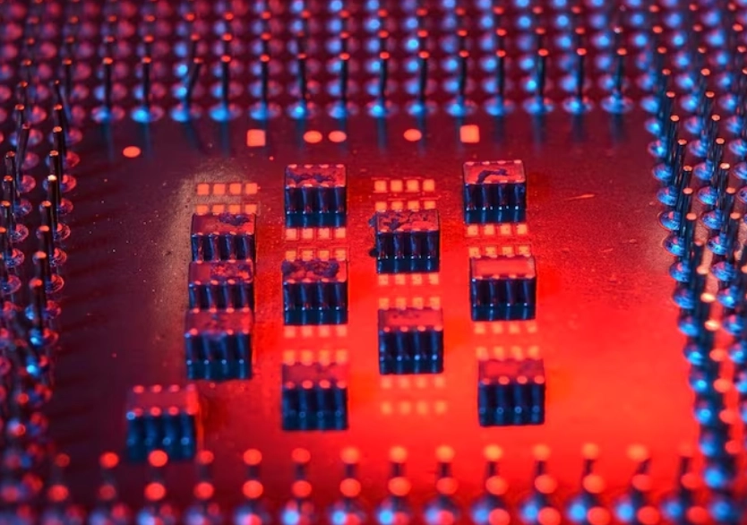
Gallium arsenide wafers rule the world of high-speed lasers and detectors. Electrons race through GaAs almost six times faster than through silicon, and its semi-insulating versions keep unwanted electrical noise extremely low. Modern factories grow perfect crystal layers only a few atoms thick so the laser color stays exactly where you want it, sometimes within one tenth of a nanometer.
Types of Optical Chips by Function
Light Emission: Transforming Electrical Signals into Photons
DFB Laser Chips for Precise Wavelength Control
A tiny built-in mirror grid forces these lasers to produce only one pure color, perfect for sending hundreds of different TV channels on a single fiber without mixing them up.
FP Laser Chips for Cost-Effective Broadband Emission
These simple lasers cost less and work great for short distances inside data centers or for cheap sensors.
VCSEL Chips Enabling High-Speed Data Links
Vertical-cavity lasers shoot light straight up from the surface, so factories can test them while still on the wafer and pack hundreds together for super-fast face-recognition or 800G connections.
Light Detection: Converting Photons Back to Electrical Signals
PIN Photodiode Chips for Standard Sensitivity Applications
A clean and fast design that turns light into current with almost no extra noise, used everywhere from 100G receivers to camera autofocus.
APD Avalanche Photodiode Chips for Low-Light Detection
These clever chips multiply every incoming photon many times inside, so you can still see the signal even after it travels 80 kilometers through fiber or bounces back from a far-away car in LiDAR.
Light Modulation: Fine-Tuning Signal Amplitude and Phase
Mach-Zehnder Modulator Chips in High-Bandwidth Systems
By splitting light into two paths and changing one path length a tiny bit with voltage, these modulators can turn digital zeros and ones into light pulses faster than 100 billion times per second.
Light Switching and Coupling: Routing Photonic Pathways
Integrated Switch Chips for Dynamic Optical Networks
Large grids of tiny mirrors or phase shifters now steer light inside the chip itself, letting giant data centers rearrange connections in microseconds.
Coupling Chips for Efficient Fiber-to-Chip Interfaces
Special tapered waveguides or grating patterns make sure almost every photon actually enters or leaves the fiber instead of bouncing away, keeping loss below 1 dB.
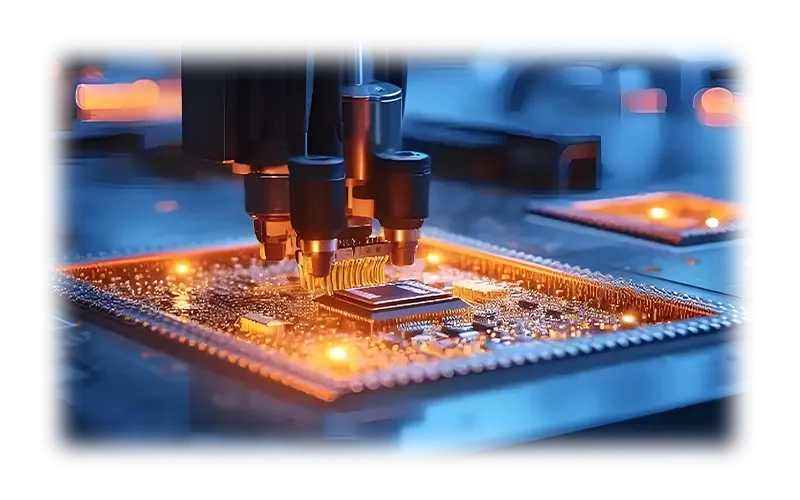
Essential Packaging Solutions for Optical Chips
Even the best laser chip will drift in color or die early if the package lets in a single drop of moisture or gets too hot. Good packaging therefore decides if your module really works for ten years in the desert or under the sea.
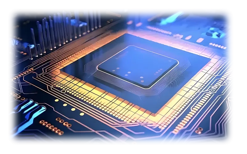
Packaging: Reliability, Thermal Control, and Miniaturization
You need perfect 50-ohm lines up to 70 GHz, heat removal better than 5 °C per watt, and airtight sealing that keeps helium leak rate under 5×10⁻⁹ atm·cc/s for decades.
DEEPETCH’s IDM Approach to Custom Optoelectronic Packaging
Because everything from ceramic design to gold plating happens in the same factory, you get prototypes in weeks instead of weeks and never worry about supply surprises.
Butterfly Packages for Laser and Detector Integration
The famous 14-pin or 7-pin metal butterfly box with built-in cooler, temperature sensor, and optical isolator is still the first choice for any serious 400G or 800G long-distance module. Many top transceiver makers simply cannot ship without it.
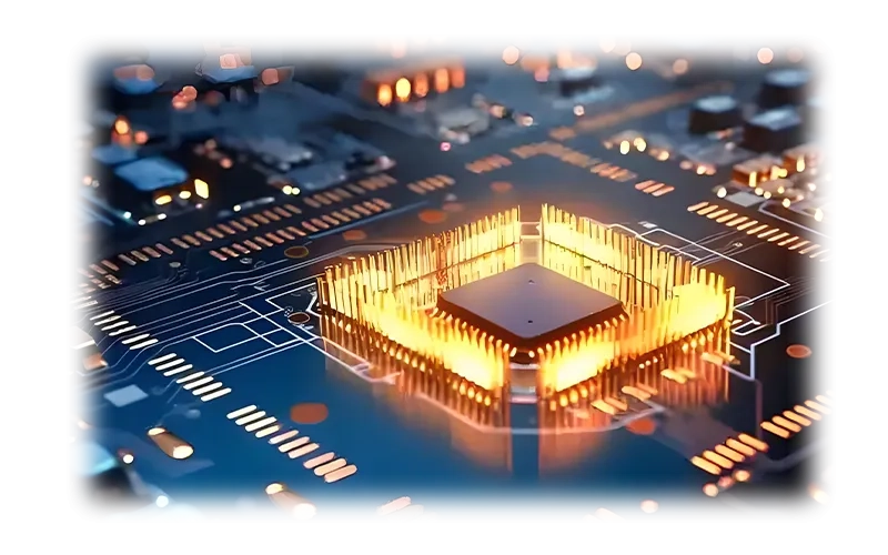
Ball Array Housing (CBGA) for Dense Interconnects
When you place lasers only millimeters away from the switch chip to save power, only ceramic BGA packages give you enough electrical pins and spread the heat fast enough.
Ceramic Pin Grid Array (CPGA) for Rugged High-Density Needs
Military and space projects love these packages because pins make replacement easy and the ceramic body survives huge temperature swings and strong vibration.
DEEPETCH’s Role in Advancing Optical Chip Ecosystems
From its clean rooms in Shenzhen, DEEPETCH has already shipped millions of packages to customers on five continents. Standard butterfly and TO types are usually in stock and ship within two weeks, while fully custom designs often reach your lab in only eight weeks.
Applications and Future Trends in Optical Chips
Telecom and Data Centers: Scaling Bandwidth with Photonic Tech
Today’s 800G and tomorrow’s 1.6T modules already use tiny InP modulators and silicon-photonic switches so one hair-thin fiber can carry the internet traffic of a small city.
Sensing and Automotive: Optical Chips in LiDAR and Beyond
Self-driving cars and drones see the world with 905 nm or 1550 nm laser chips packed in tough automotive-grade packages that survive rain, salt, and −40 °C winters.
Emerging Frontiers: Quantum Optics and 3D Integration
New quantum-dot lasers and super-thin lithium niobate modulators promise another big jump in speed and power saving in the next five to ten years.
Partner with DEEPETCH for Your Optical Chip Journey
Optical chips have grown from curious lab toys to the beating heart of global internet and AI. Your success now depends not only on choosing the right laser or detector chip, but also on finding a packaging partner you can truly trust. With proven butterfly packages, ceramic BGA, CPGA platforms, and full in-house IDM ability, DEEPETCH gives you one reliable partner from first sketch to million-unit production.
FAQ
Q1: Why do people still use gallium arsenide instead of cheap silicon for optical chips?
A: Gallium arsenide lets electrons turn directly into light very easily because of its direct bandgap, while silicon needs complicated extra steps and still wastes more power.
Q2: Why can’t we just use plastic packages like phone chips?
A: Lasers change their color if temperature moves even one degree, and a single water molecule inside can kill them in months. Only metal or ceramic hermetic packages keep them alive for twenty years in real networks.
Q3: When should you pick a butterfly package?
A: Pick it whenever you need a built-in cooler, perfect 50 GHz signals, and an optical isolator, basically every 100G+ long-reach or coherent module.
Q4: Are ceramic BGA packages really ready for putting lasers next to AI chips?
A: Yes, they handle over a thousand connections, pull heat away fast, and match the expansion of silicon so nothing breaks when it gets hot.