Etch precision defines your fab’s success. One micron of non-uniformity can scrap an entire wafer. Ion source grids solve this by shaping plasma into razor-sharp beams that remove material exactly where needed. Yield climbs when grids maintain beam collimation across 300 mm surfaces. Efficiency rises as cycle times shrink without redeposition. You need substrates that endure ion bombardment without flaking or charging. DEEPETCH delivers exactly that. Their IDM model controls every step from crystal growth to final polish. Explore IDM capabilities for custom runs. Substrates arrive etch-ready, letting grids perform at peak.
What Are Ion Source Grids and How Do They Work in Etching?
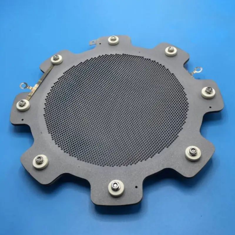
Three perforated plates float inside the etch chamber. The first extracts ions. The second accelerates them. The third focuses the beam. This stack turns chaotic plasma into a disciplined cutting tool.
Ion Beam Generation and Grid Functions
Argon gas ionizes between cathode and anode. Electrons collide, spawning positive ions. The screen grid sits at plasma potential. Apertures as small as 0.5 mm let ions stream through. Voltage gaps between grids set beam energy from 50 eV to 2 keV.
Precision Patterning Mechanisms
Each aperture acts like a lens. Beamlets merge downstream into a uniform sheet. Incidence angle stays 90 degrees, preventing sidewall taper in 20:1 trenches. Molybdenum grids resist erosion for 5,000-hour campaigns.
Role in Reactive and Physical Etching
Fluorine radicals ride the beam in reactive mode. They attack silicon nitride selectively. In physical mode, argon ions sputter gallium arsenide. Grid alignment keeps etch rate variation below 1% across the wafer.
How Do Ion Source Grids Prevent Yield Loss During Etching?
Beam divergence above 2 degrees creates shadows. Particles redeposit and mask features. Dies fail. Grids stop this with laser-drilled aperture arrays aligned to 5 μm.
Uniform Beam Distribution Control
Self-aligned grids use ceramic spacers. Ion flux stays flat from center to edge. Etch depth varies less than 3 nm on monocrystalline silicon substrates pulled by Czochralski method. Defect density drops under 0.1/cm².
Surface Damage Minimization
Low-energy extraction at 100 eV limits lattice disruption. Silicon surfaces stay mirror-smooth. No amorphization layers form. Your post-etch cleans become faster.
Monocrystalline Silicon Substrate Synergy
Single-crystal lattices guide ion trajectories. No grain boundaries scatter beams. Yield on 3 nm nodes reaches 92% when grids pair with these substrates.
What Are the Biggest Challenges in Maintaining Etching Consistency?
Grids erode. Apertures widen. Beam focus drifts. Thermal cycles crack insulators. Contamination from sputtered metal poisons plasma.
Grid Erosion and Contamination Risks
Molybdenum sputters at 1 μm per 100 hours under fluorine. Particles land on wafers. Shorts form. Cleaning intervals shrink to daily.
Thermal and Electrical Stability Issues
Grid temperature swings 200 °C during cycles. Differential expansion misaligns plates. Arcing burns holes.
Zinc Oxide Wafer Integration Solutions
Transparent conductive layers on zinc oxide wafers absorb stray charge. Plasma stays stable. Grid life extends 30%. Etch uniformity holds at 98.5% across 200 mm surfaces.
How Can Ion Source Grids Reduce Etching Cycle Time?
Cycle time dictates throughput. Faster extraction means more wafers per hour. Lower power cuts utility costs.
Accelerated Ion Extraction Techniques
Double-grid stacks raise extraction field to 5 kV/cm. Beam current doubles without divergence. Etch rate on alumina hits 500 nm/min.
Lower Energy Consumption Profiles
RF power drops 15% when grids match substrate impedance. Heat load on chillers falls. Your fab saves 200 kWh per shift.
Alumina Ceramic Substrate Optimization
High thermal conductivity of 30 W/m·K spreads heat. Grid temperature stabilizes. Cycle time shortens 12% on alumina platforms.
Why Is Material Compatibility Critical for Grid Performance?
Mismatched substrates charge under ion flux. Beams deflect. Patterns shift. Select materials that stay neutral.
High-Temperature Endurance Requirements
Grids reach 400 °C during oxide etch. Substrates must not outgas or warp. Silicon nitride holds shape to 1,200 °C.
Chemical Resistance Standards
Fluorine attacks silicon dioxide. Nitride layers resist 1,000:1 etch selectivity. No pinholes form.
Silicon Nitride Substrate Advantages
Dense CVD films block ion penetration. Charge buildup stays under 2 V. Beam stability lasts entire batch on silicon nitride surfaces.
What Innovations Are Driving Next-Gen Etching Efficiency?
Multi-grid stacks and smart controls lead the charge. AI predicts erosion patterns before they impact yield. Real-time adjustments keep beams tight and uniform.
Multi-Grid Architecture Advances
Four-plate systems add focusing lenses between extraction and deceleration stages. Beam divergence falls to 0.5 degrees. Aspect ratios climb past 50:1 on gallium arsenide and silicon carbide wafers. Etch profiles stay vertical even at 100:1 depths.
Smart Process Monitoring Integration
Embedded sensors track aperture wear in situ. Software tweaks voltages on the fly. Beam current stabilizes within 0.5%. Downtime drops 40%. Predictive maintenance schedules replace grids exactly when needed.
DEEPETCH In-Stock Chip Compatibility
Ready substrates arrive pre-qualified for grid alignment. Swap in new lots without recalibration. Your line runs uninterrupted. Lead times shrink to 48 hours for standard grades.
FAQ
Q1: How do ion source grids affect etch uniformity?
A: Grids collimate beams to 1-degree incidence. Apertures align within 5 μm across the stack. Ion flux spreads evenly from center to edge. Etch depth varies less than 1% across 300 mm wafers. Center-to-edge non-uniformity drops below 0.8% on monocrystalline silicon.
Q2: Which substrate best resists grid-induced charging?
A: Silicon nitride stays neutral under 2 keV bombardment. Dense CVD films block charge migration. Surface potential rises only 1.5 V. Beam deflection stays below 0.2 degrees. No arcing occurs even at 10¹³ ions/cm² fluence.
Q3: Can grids reduce power consumption in etching?
A: Optimized extraction fields cut RF power 15%. Double-grid geometry raises efficiency to 85%. Each eight-hour shift saves 200 kWh. Chiller load falls 12% as waste heat decreases.
Q4: What grid material lasts longest in fluorine plasma?
A: Molybdenum endures 5,000 hours before aperture growth exceeds 5%. Sputter yield stays at 0.3 atoms/ion. Surface roughening remains under 50 nm. Grid replacement intervals extend 40%.
Q5: How quickly can you source etch-grade substrates?
A: In-stock lots ship within 48 hours. Standard grades leave the warehouse same-day. Custom runs start in two weeks. Qualification data ships with every batch.