CDIP continues to play a crucial role in the field of extreme environment electronics due to its irreplaceable reliability. Although it faces competition from miniaturized packaging (QFN) in the future, it is expected to open up new tracks in high-end sectors such as aerospace, deep space exploration, and supercomputing through material innovation (aluminum nitride) and system-level integration, becoming a key component of the high-value-added electronics ecosystem.
- Core advantages of CDIP packaging
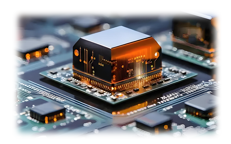
CDIP (CERAMIC DUAL INLINE PACKAGE) is a double row straight plug package using ceramic materials (alumina AL₂O₃ or aluminum nitride ALN) as the tube shell. Compared with plastic package (PDIP) and metal package, it has the following significant advantages:
- High reliability and long life
High temperature resistance: ceramic materials can withstand extreme temperatures (55°C to 200°C and above), suitable for high temperature welding processes (reflow soldering), extreme environments (aerospace, military).
Excellent airtightness: sealed by glass or metal, moisture-proof and oxidation-proof, in line with MILSTD883 airtightness standard, leakage rate less than 5×10⁻⁸ ATM·CC³/SEC.
Anti-mechanical stress: The ceramic structure is strong and has better seismic performance than plastic packaging (PDIP), which is suitable for vibration environment.
- High frequency and electrical performance advantages
Low dielectric loss: the dielectric constant of alumina ceramic (~9.8) is lower than that of epoxy resin (~4.5), suitable for high frequency microwave circuits (radar, communication modules).
Electromagnetic shielding: The metallized layer can provide EMI protection and reduce signal interference.
High insulation resistance (> 10¹² Ω): reduces leakage current and is suitable for high precision analog circuits
- Environmental adaptability
Chemical corrosion resistance: acid and alkali resistant, salt spray resistant, suitable for chemical or Marine environment (oil drilling sensors).
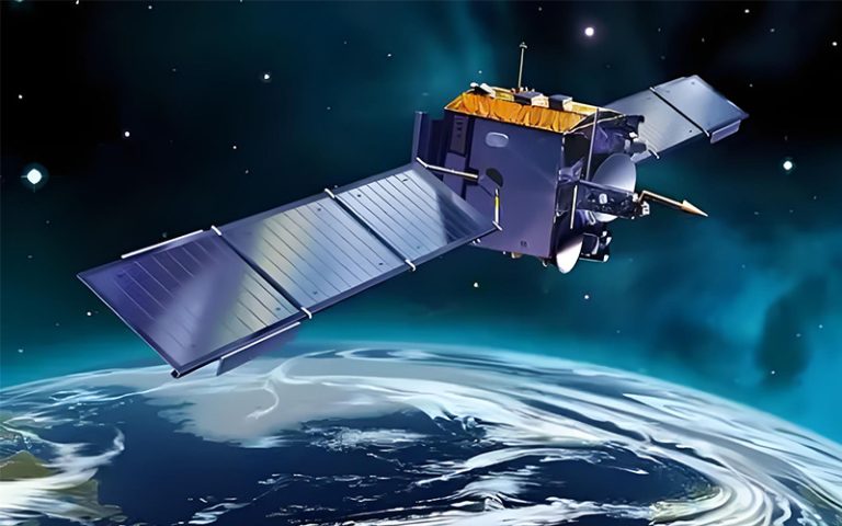
Radiation tolerance: some doped ceramics can resist space radiation and be used in satellite electronic devices
High mechanical strength: strong resistance to impact and vibration, suitable for vehicle and industrial equipment.
Excellent thermal conductivity (AL₂O₃: 2030 W/M·K; ALN: 150200 W/M·K): efficient heat dissipation through metal pins or heat sinks.
- The most prominent technical indicators in industrial applications
The core technical indicators of CDIP determine its irreplaceability in the high-end field:
| qualification | Typical values/characteristics | Application impact
| gas tightness | Leakage rate <1×10⁸ ATM·CC³/SEC (helium inspection) | Ensure high reliability and suitable for aerospace and military
| Thermal expansion coefficient (CTE) | 6-8 PPM/°C (matched to silicon chip) | Reduce thermal stress and improve welding reliability
| Dielectric constant (DK) | 9-10 (AL₂O₃) | Affects high frequency signal integrity (<5GHZ applicable)
| Number of pins | 8-64 pins | Suitable for medium and high complexity IC packaging
| Packaging size | Standard DIP spacing 2.54MM | Compatible with traditional PCB through-hole insertion process
| temperature | 55°C to + 175°C (military standard) | Civilian grade can reach 40°C to +125°C
| thermal resistance | Typical value 3550°C/W | Support higher power chips
- Compare other packaging types:
PDIP (plastic DIP): low cost but poor temperature resistance (40°C to +125°C) and poor gas tightness.
Metal packaging (TO type): better heat dissipation, but limited number of pins (usually up to 12).
Life prediction: MTBF (mean time between failures) is calculated by ARRHENIUS model to be over 100,000 hours
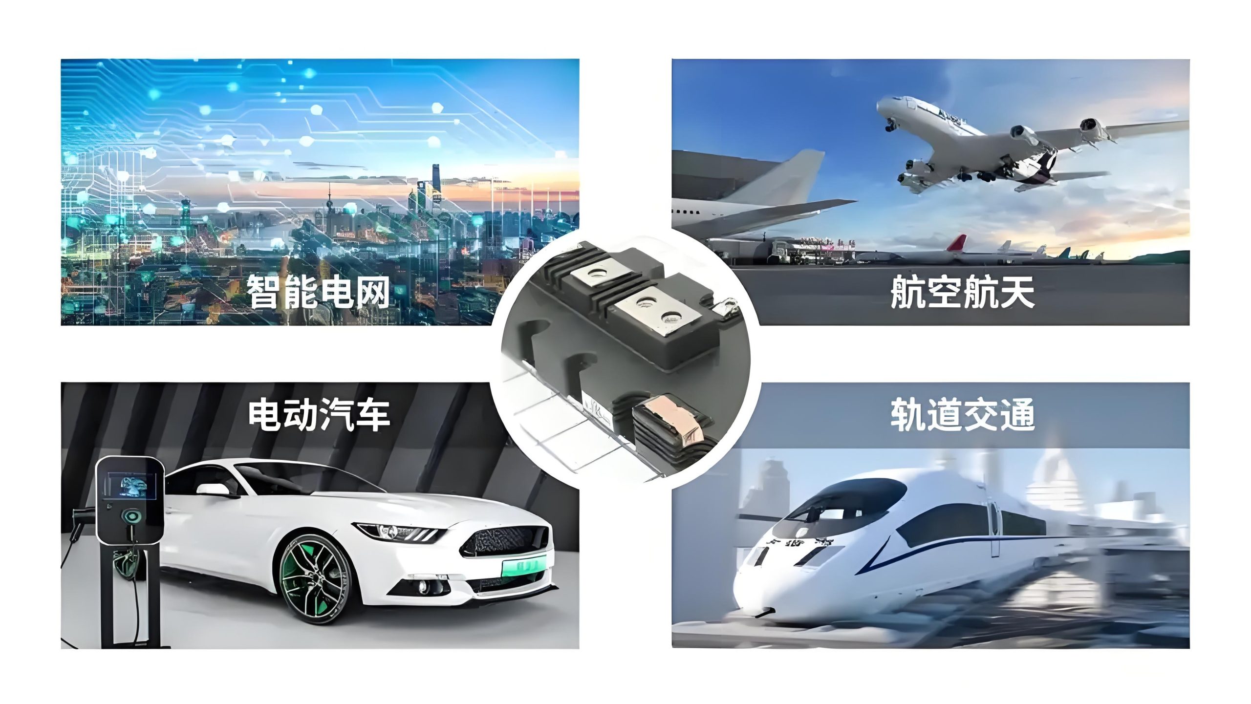
- Special application scenarios
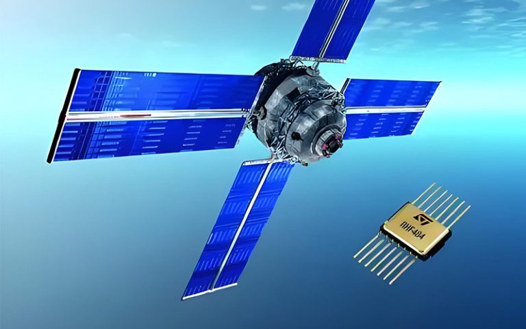
- Aerospace and military industry
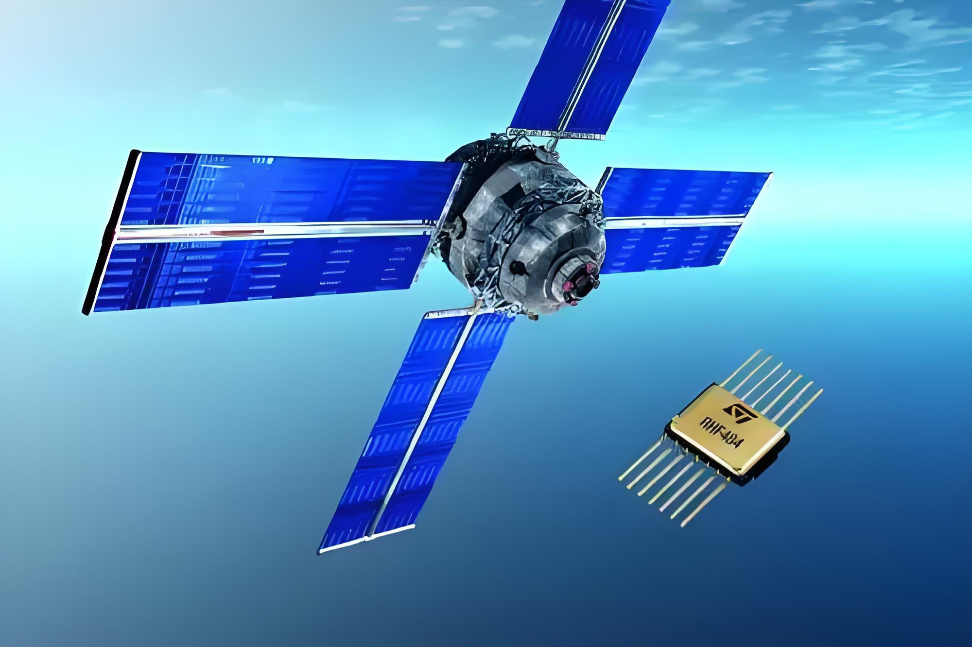
IC packaging for satellite and missile guidance systems (radiation resistant, extreme temperature resistant).
Military communication module (high frequency, low loss requirements).
- Automotive electronics (high reliability scenarios)
High temperature resistant packaging of engine control unit (ECU) and sensor (oxygen sensor).
Electric vehicle power module (ALN based CDIP for IGBT drive).
Industry and energy
Oil drilling equipment (anti-vibration, corrosion resistant).
Power electronic devices (relays, optocouplers) under high pressure/high temperature environment.
- Medical and longevity equipment
Implantable medical devices (pacemakers, need airtightness and biocompatibility).
Industrial automation control module (more than 10 years of life requirement).
- Future development trends
Material upgrade
Aluminum nitride (ALN) as an alternative to alumina: improves thermal conductivity (200 W/M·K) and is suitable for higher power density devices.
3D printing technology: rapid forming of ceramic tubes and shells, reducing the cost of small batch customization
Low temperature co-fired ceramics (LTCC): integrated passive components (resistors/capacitors), reducing the size of peripheral circuits.
- Miniaturization and high density
Multilayer ceramic substrate: integrated passive components (LTCC technology) to reduce peripheral circuits
Narrow pitch CDIP (pin pitch <1.27MM): Suitable for high pin count requirements and partially replaces QFP packaging.
3D stacked CDIP: multi-layer interconnection through ceramic intermediate layer to improve integration.
- Expansion of emerging markets
Quantum computing: Superconducting devices need to be packaged in an environment with extremely low thermal expansion and vacuum sealing.
Space commercialization: The demand for high reliability packaging of low cost satellites (STARLINK) is growing.
- Environmental adaptability upgrading
Radiation enhancement: yttrium-doped ceramics for low-Earth orbit satellites (total radiation resistance> 100 KRAD).
Ultra high pressure packaging: deep sea detector pressure resistant shell (> 1000 atmospheres) and electronic packaging integrated design


