


The SCH Series is a high-performance DAF/DDAF (Die Attach Film) designed to streamline and enhance the advanced packaging process....

The DEEPETCH DP-QPA2611 is a high-performance X-Band (8–12 GHz) Gallium Nitride (GaN) Power Amplifier...

The DEEPETCH DP-ROS-40121 is a premium, solvent-free epoxy die attach adhesive engineered for the most...
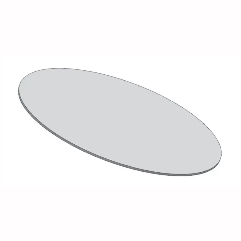
The Diamond Heat Spreader is a highly efficient thermal management material engineered for the most demanding...
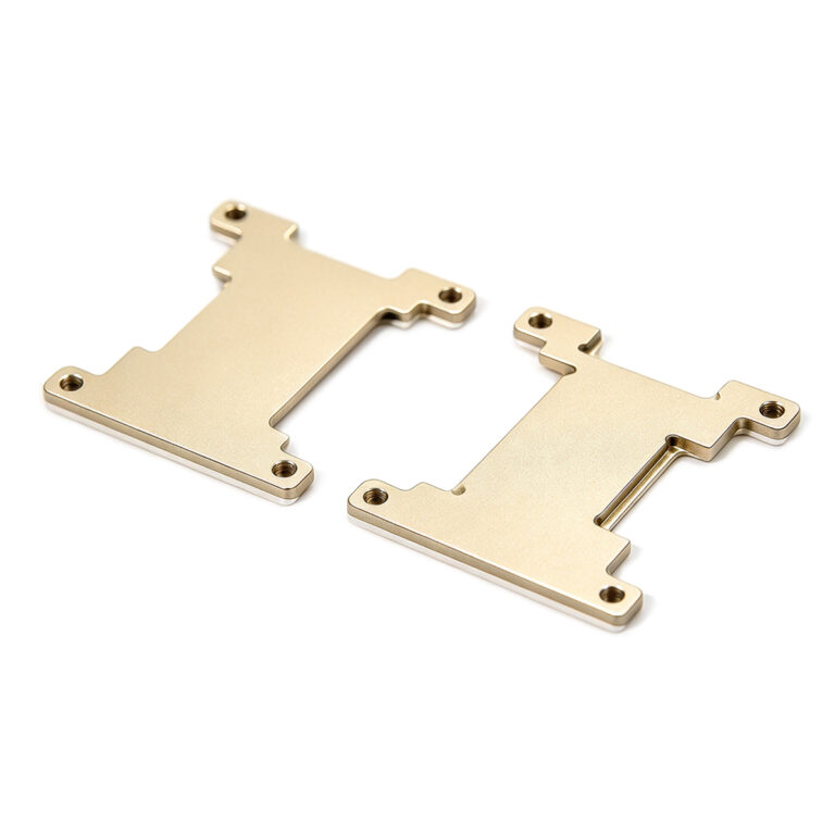
Molybdenum copper composite: adjustable CTE, high conductivity, lower density than tungsten copper. No...
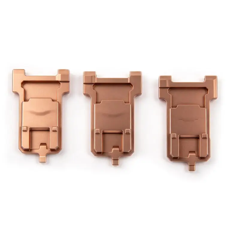
Tungsten copper composite: low CTE, high conductivity. Ideal for RF, power, optical packaging.
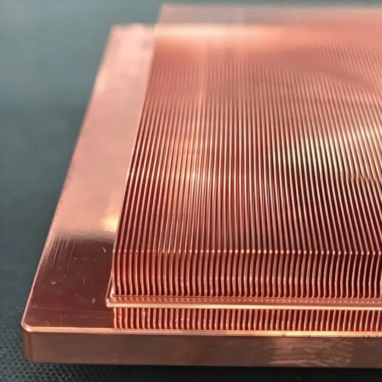
Diamond-Copper Thermally Conductive Composite. High thermal conductivity, tunable CTE, robust.
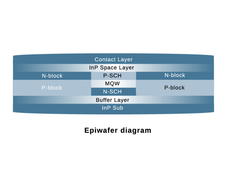
The DE-CW-1310 DFB EPI wafer, a high-performance epitaxial structure designed for distributed feedback (DFB) lasers operating at 1310 nm....
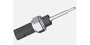
Ceramic thin-filmvacuum sensor Optical gas massflowmeter Liquid mass flowmeter Force sensor MEMS...
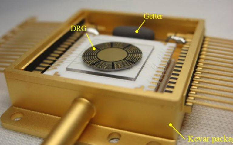
Photoelectric sensing chip Light source chips Optical transmission and modulationchips Optical detection and receptionchips...