The move to Wide-Bandgap (WBG) semiconductors represents a key shift in power electronics today. Higher efficiency and reduced size in power conversion systems come from Silicon Carbide (SiC) and Gallium Nitride (GaN), which outperform traditional silicon in switching speed and energy loss. Yet, heat builds up in smaller areas, posing a major design challenge. Thermal management now forms the base for reliable operation and performance under tough conditions.
The Thermal Imperative in Wide-Bandgap Power Systems
Adopting WBG materials demands a basic rethink of heat removal methods. Although these devices handle higher power levels in less space, the area for heat escape narrows. This situation can cause even efficient chips to overheat if the heat route to the surroundings faces blocks. The thermal link must rank as a vital part of the overall electrical setup.
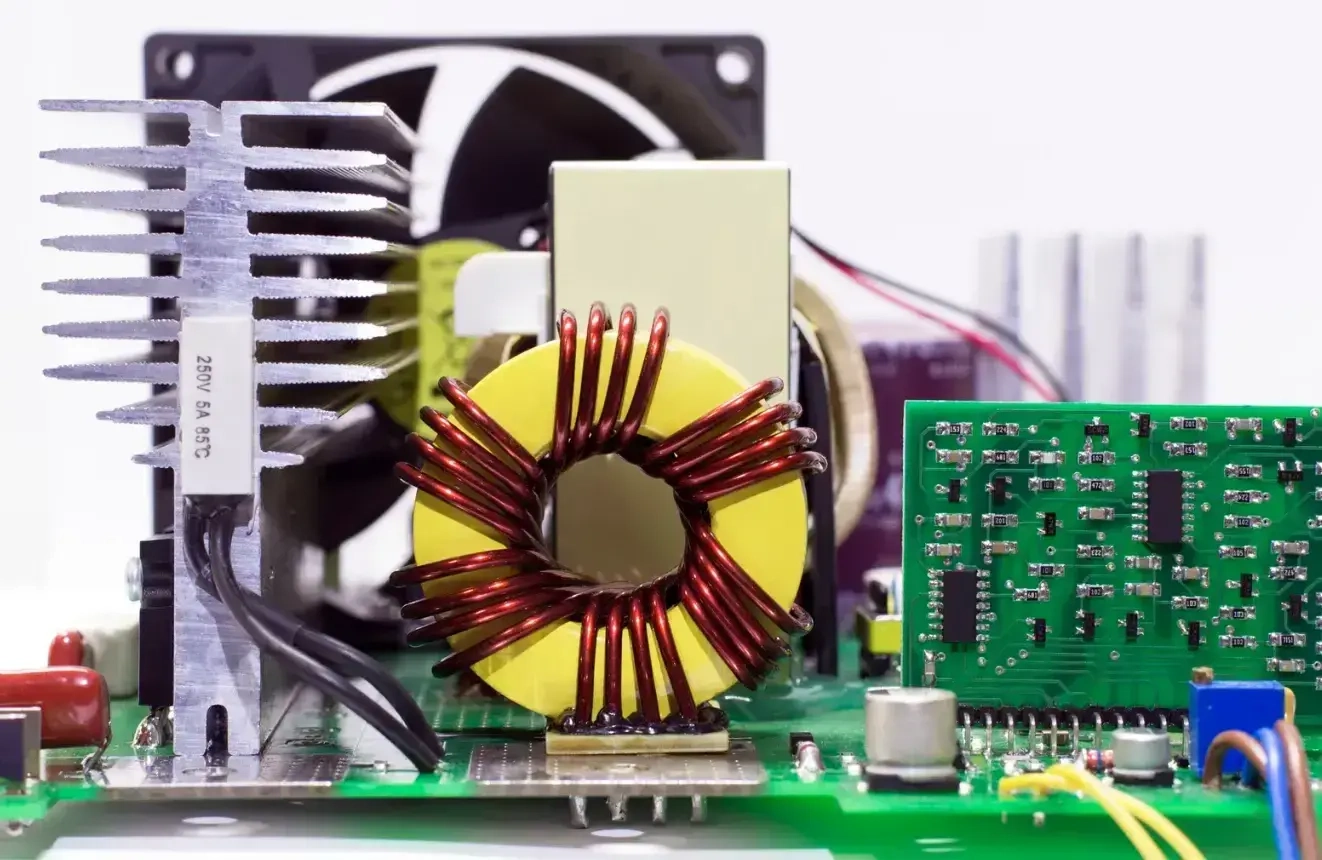
High Power Density Challenges
Power modules today fit more features into smaller areas, which creates focused heat flow beyond basic cooling limits. Designs with tight layouts face thermal resistance from the chip junction to the housing as the main limit on power handling. Such resistance hampers overall system capacity when heat builds rapidly.
Material Property Advantages
SiC shows much better thermal conductivity than silicon, so heat spreads across the device more readily. GaN provides strong electron movement, which supports smaller units that produce less heat in fast switching, as long as the base material manages the focused load. These traits allow both materials to excel in compact, high-demand setups.

Reliability and Longevity Impacts
Too much heat speeds up issues like wire movement and oxide failure in gates. Keeping temperatures in check through careful thermal planning helps power systems last as planned, particularly in key areas such as industry or vehicles. Proper control thus preserves device health over extended use.
Innovative Cooling Strategies for SiC-Based Applications
SiC technology shines in high-voltage and high-temperature roles, but cooling must go past simple sinks to fully tap its strengths. Standard solder links often break under the heat where SiC works best, so advanced bonding and cooling approaches become essential. These methods ensure the device stays functional in demanding power tasks.
Advanced Packaging Materials
Ceramic bases with high conductivity, such as Silicon Nitride (Si3N4), or silver bonding in place of regular solder cut down thermal barriers greatly. These options deliver the durability required for repeated heat shifts in tough power uses. As a result, they support longer operation without failure.
Active Liquid Cooling
Air-based cooling falls short for strong inverters, where liquid methods directly on the chip or through fine channels pull away large heat volumes from the base. This keeps SiC MOSFETs in their best temperature range even under full load. Such systems maintain steady performance in high-output scenarios.
DEEPETCH SiC Solutions
DEEPETCH stands as a leader in semiconductors since 2019, following an IDM (Integrated Device Manufacturing) approach that oversees design and production fully. This setup yields SiC items with top performance and built-in heat release from the start, serving over 1,560 customers worldwide. Their solutions fit data centers and AI systems, where heat control proves critical for uptime.
Solving Thermal Constraints in High-Frequency GaN Designs
GaN units suit fast-frequency tasks well, yet their compact form turns heat removal into a fine-tuned process. In surface-mount setups common for Gallium Nitride (GaN), the circuit board acts as the main heat spreader. Board planning must avoid hot areas that disrupt nearby signal parts. Careful layout thus safeguards overall function.
Parasitic Inductance Minimization
Thermal and electrical routes in GaN setups link closely, so low-inductance packages boost switching while cutting heat from unwanted vibrations. Devices then run at higher speeds with less warmth. This balance enhances efficiency in frequency-heavy applications.
Surface Mount Thermal Vias
Thermal vias under the GaN pad form a grid that channels heat via copper paths through board layers to ground or outer spreaders. They overcome the poor heat flow of FR4 material effectively. As such, they keep the chip cool in mounted designs.
DEEPETCH GaN Performance
DEEPETCH GaN products handle tight power supply needs through deep etching and thin-film methods, yielding FETs with low resistance and better heat routes. These traits make them suitable for dense power units in future systems. Reliability follows from this optimized build.
Industrial and Military Standards for Thermal Reliability
Harsh settings test electronics beyond heat alone, including gases, moisture, and shakes. Standards like IPC-Class 3 or AEC-Q for vehicles confirm that thermal plans endure without harming the chip core. Compliance ensures steady work in extreme cases.
Automotive Grade Qualifications
Parts in vehicle drives endure many quick heat changes, so WBG items undergo tests to check bonds and covers against peeling in cold-to-hot shifts. Strong materials prevent such breaks during operation. This testing upholds safety in motion.
Aerospace Vacuum Requirements
Space or high flights lack air for cooling, relying on direct heat transfer and glow instead. Low-gas thermal pads and high-glow covers become key choices for design. They enable function where other methods fail.
Comprehensive Quality Control
Under the Integrated Device Manufacturing (IDM) model, firms like DEEPETCH apply strict systems such as IATF 16949 and ISO 9001. Every chip faces trait checks and environment tests for harsh-world performance. This process guarantees robust outcomes.
Why Partner with DEEPETCH for Your Next Generation Design
Selecting suppliers goes beyond specs to secure steady chains and full oversight. Partners handling chip lifecycles offer clear views and tweaks that others lack, especially for WBG heat challenges. Such ties aid complex builds.
IDM Strategic Advantage
IDM lets quick changes in designs to fix heat problems, adjusting films or packs if needed for specific uses. In-house making supports these shifts smoothly. Results meet unique thermal demands better.
Robust Supply Chain
DEEPETCH holds large stocks of Chips in Stock, cutting delays from worldwide moves. Access supports prototypes and full runs on time. Projects advance without holdups.
Global Engineering Support
Knowledge in heat flow, tiny structures, and signals enables full system planning. Global aid refines heat models and picks fitting SiC or GaN for goals and costs. This guidance boosts design success.
FAQ
Q1: Why is SiC preferred over Silicon for high-temperature environments?
A: SiC has a wider bandgap and much higher thermal conductivity than silicon, allowing it to operate reliably at temperatures exceeding 200°C while maintaining efficient heat transfer away from the junction.
Q2: How does the IDM model benefit thermal management in power electronics?
A: The IDM model enables the manufacturer to optimize the entire device architecture, from the internal chip layers to the final packaging, ensuring the most efficient thermal path is built into the product from the start.
Q3: Can GaN devices be used in liquid-cooled systems?
A: Yes, GaN devices are frequently integrated into liquid-cooled designs, particularly in high-density power converters for EVs and data centers, where active cooling is needed to manage concentrated heat.
Q4: What role do thermal vias play in GaN PCB design?
A: Thermal vias act as vertical heat pipes, carrying thermal energy from the GaN chip through the insulating PCB layers to larger copper planes or external heat sinks, which is crucial for surface-mount components.