The shift toward 3D and 2.5D semiconductor integration is not just a technological trend—it’s a restructuring of how chips are packaged, interconnected, and cooled. These packaging architectures push the limits of design density, power efficiency, and thermal management. In this landscape, even a few microns of misalignment during assembly can compromise performance. That is where ultra-precise packaging equipment becomes non-negotiable.
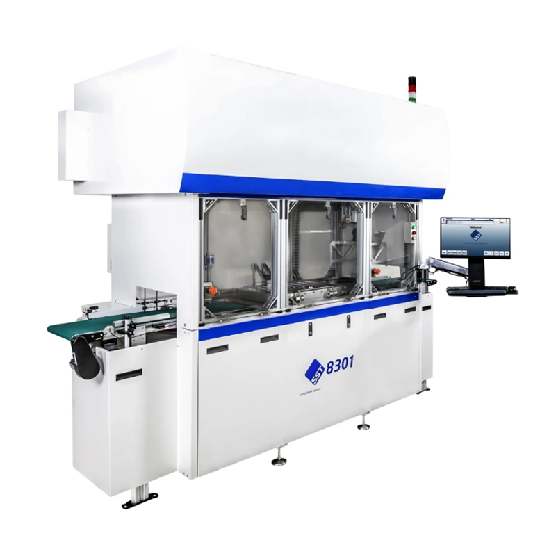
DEEPETCH, a specialized manufacturer with years of experience in ceramic semiconductor packaging equipment, operates with a focus on high-precision assembly solutions for industries where failure is simply not an option. The company’s offerings cover a complete set of ceramic IC packaging lines—compatible with CDIP, CQFP, CBGA, CLCC, and more—designed to meet the demanding requirements of aerospace, defense, automotive electronics, and high-reliability communication systems.
What Role Does Packaging Equipment Play in 3D and 2.5D Integration
Before talking about micron-level tolerances, it’s worth understanding the role of packaging equipment in these advanced integration schemes. In 3D integration, multiple dies are stacked vertically, connected through through-silicon vias (TSVs) or micro-bumps. In 2.5D, chips sit side-by-side on an interposer that acts as a high-speed communication bridge.
Enabling High Interconnect Density
For both architectures, interconnect density is the name of the game. As die sizes shrink and I/O counts soar, the packaging stage must handle layouts with thousands of solder joints, each placed within a few microns of accuracy. DEEPETCH’s equipment—drawing from its ceramic packaging experience—uses high-precision servo systems and optical alignment cameras capable of positioning to within ±5 μm. This capability ensures that dense ball-grid arrays and fine-pitch leads are connected without electrical shorts or open circuits.
Maintaining Thermal and Mechanical Stability
In advanced integration, temperature cycling is not gentle. Devices in an automotive engine control unit, for example, may swing from −40 °C to +125 °C repeatedly. The combination of ceramic substrates and DEEPETCH’s controlled bonding processes ensures minimal coefficient of thermal expansion (CTE) mismatch between components, which reduces warpage and long-term mechanical fatigue.
Reducing Defect Rates in Complex Assemblies
The more dies and interconnects in a package, the more chances for defects. A single micro-bump misalignment can render a high-value 3D stack useless. DEEPETCH integrates inline AOI (Automatic Optical Inspection) and solder paste inspection systems to detect such issues immediately, allowing rework before the package is sealed. This approach—common in mission-critical electronics—saves both material cost and production time.
Why Is Ultra-Precision Critical in Advanced Packaging
As packaging geometries tighten, the margin for error evaporates. You can think of it like parking a truck in a space just centimeters wider than the vehicle—it can be done, but only with guidance and constant checks.
Tolerance Requirements in Micron Scale
For many 2.5D interposers, misalignments beyond ±5 μm can lead to electrical impedance shifts or even shorts. In some high-frequency RF applications—common in aerospace radars—tolerances are even stricter. DEEPETCH designs its pick-and-place heads with sub-micron incremental control, ensuring repeatability over long production runs.
Alignment Systems with Real-Time Feedback
Precision is not just about the machine’s first move—it’s about maintaining it across hours of operation. DEEPETCH’s packaging lines use real-time vision alignment systems with feedback loops, correcting for drift due to machine wear or thermal changes. This is especially important in ceramic packaging, where firing processes can slightly alter substrate dimensions.
Impact on Signal Integrity and Yield
Poor mechanical alignment is not just a visual defect—it affects electrical pathways. Misaligned interconnects may create extra parasitic capacitance or delay, undermining the speed advantages that 3D/2.5D integration promises. DEEPETCH’s consistent alignment precision directly correlates to higher yields and stable high-frequency performance.
How Does DEEPETCH Packaging Equipment Meet These Demands
DEEPETCH’s strength lies in combining traditional ceramic packaging expertise with automation technologies that fit modern semiconductor roadmaps. DEEPETCH is also certified with strict quality control systems that align with both domestic and international semiconductor manufacturing standards.
Integration with Ceramic Packaging Lines
Their packaging systems are built to integrate seamlessly into ceramic assembly lines—handling CDIP, CQFP, CBGA, CLCC packages without switching tooling. This flexibility allows one line to produce multiple package types, a clear advantage for manufacturers serving both legacy and advanced markets.
Automated Pick-and-Place with High Accuracy
Servo-driven pick-and-place modules equipped with vacuum handling heads achieve consistent force control, avoiding die cracks or solder joint stress. These systems operate at high throughput while maintaining accuracy—essential for scaling production without compromising quality.
Process Monitoring and Quality Control Features
Built-in monitoring for process temperature, bonding force, and environmental humidity ensures that each package meets its target specification. The inclusion of AOI systems after each major assembly step gives operators immediate feedback, minimizing downstream rejections.
What Are the Key Benefits for 3D and 2.5D Applications
The benefits of such equipment go far beyond simple “better alignment.”
Enhanced Reliability for Mission-Critical Electronics
In aerospace satellites or military radar systems, a single defective package can mean mission failure. DEEPETCH’s adherence to military and space-grade ceramic packaging standards ensures reliability even under radiation exposure or vacuum conditions.
Compatibility with Multiple Substrate Types
While ceramic is a DEEPETCH specialty, the same platforms handle organic and hybrid substrates, giving semiconductor makers the flexibility to adapt to changing BOM requirements.
Scalability for Volume Production
The transition from pilot runs to full-scale production is often where precision suffers. DEEPETCH equipment maintains tolerances and throughput across these shifts, supporting long-term contracts without costly line requalification.
Where Will Packaging Equipment Technology Go Next
The roadmap for packaging equipment is closely tied to semiconductor integration trends.
AI-Assisted Process Control
Process optimization is increasingly data-driven. DEEPETCH is exploring machine-learning algorithms to adjust pick-and-place speeds, bonding pressures, and heating profiles in real time, based on historical defect data.
Higher Throughput without Precision Loss
New motion control systems and improved vision processing speeds will allow equipment to handle more units per hour without sacrificing micron-level accuracy.
Integration with Smart Factory Systems
The next decade will see packaging lines more deeply integrated into MES systems, enabling predictive maintenance, automated traceability, and faster changeovers between product types.
FAQ
Q1: What makes ultra-precise equipment essential for 3D integration
A: In stacked and interposer-based designs, even tiny misalignments can disrupt performance. Ultra-precise tools keep alignment consistent throughout the process.
Q2: Can these systems work with both ceramic and organic substrates
A: Yes, DEEPETCH equipment supports ceramic, organic, and hybrid substrates, giving manufacturers versatility in production planning.
Q3: How does automation improve yield in advanced packaging
A: By reducing human intervention and integrating inspection at each stage, automation keeps defects from propagating through the production line.