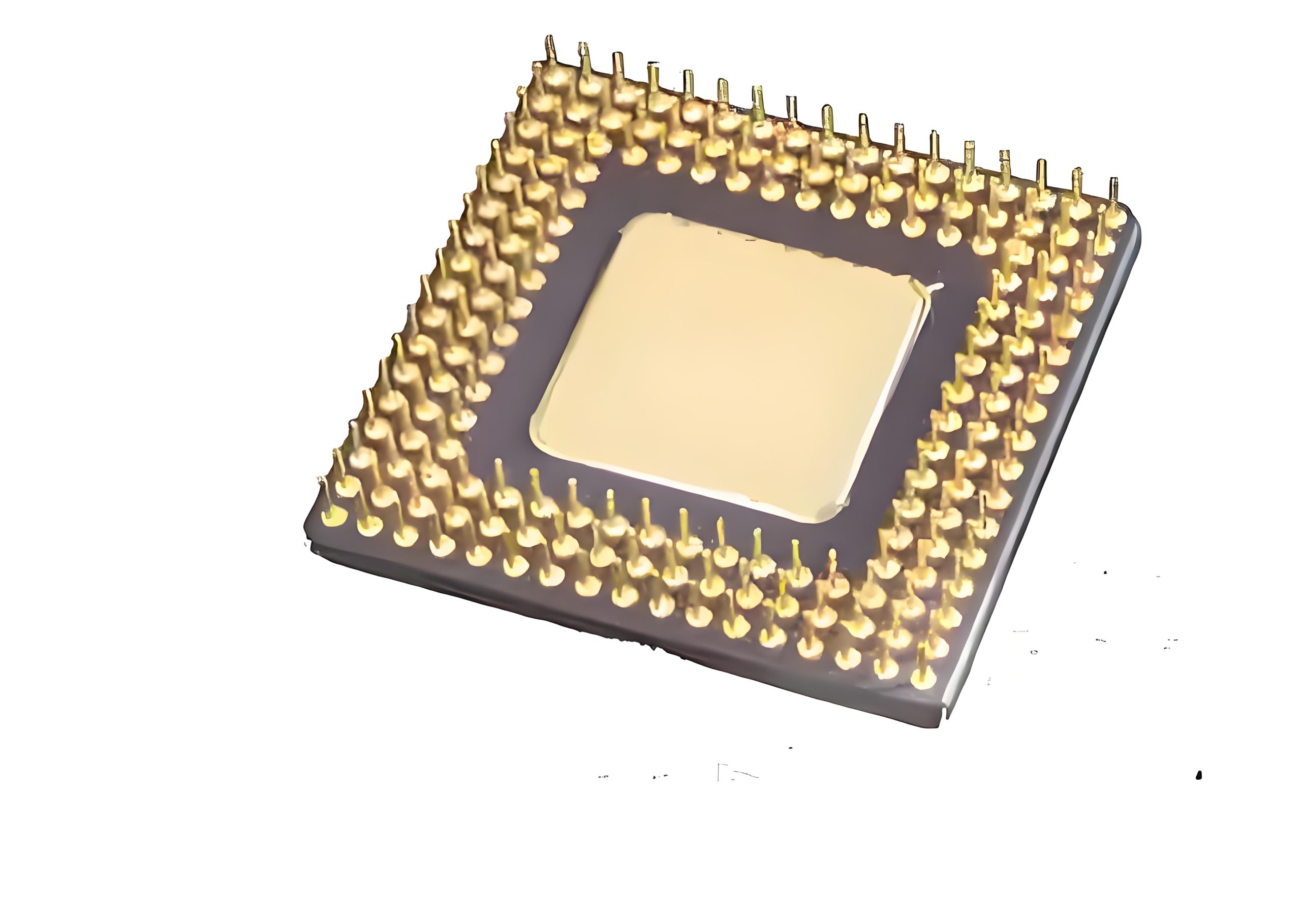
The core material of the BT resin (bismaleimide triazine resin) substrate is a copolymer of bismaleimide (BMI) and triazine resin. It is typically formed through a copolymerization reaction between cyanate ester resin and BMI at high temperatures (170-240°°C), with modifiers such as epoxy resin, polyphenylene oxide (PPE), or allyl compounds added to optimize performance. This material serves as the base for manufacturing packaging substrates.
- Material composition of BT resin substrate
- Resin system
Bismaleimide (BMI): Provides high heat resistance (TG> 200℃)
Triazine resin: improved dielectric properties (DK = 3.84.2)
Modified epoxy resin (part formula): enhanced adhesion and toughness
- Reinforced materials
EGLASS Fiber cloth: standard type (thickness 50200ΜM)
Ultra-thin glass fiber cloth/nonwoven fabric: used for thin substrate (<100ΜM)
- Conductive materials
Rolling copper foil (RA copper): 1835ΜM thick, high ductility
Low profile electrolytic copper foil (LP copper): suitable for fine lines
- Functional additives
Inorganic filler (SIO₂/ALN): adjust CTE (1216PPM/℃)
Fire retardants (phosphorus/nitrogen): meet UL94 V0 standards
- Manufacturing process of BT resin substrate
- Copper clad plate (CCL) preparation
- Resin glue preparation: BMI + triazine resin + solvent mixture
- Fiberglass cloth impregnation: control the resin content (4060WT%)
- Semi-cured sheet (PREPREG): BSTAGE pre-cured
- Laminated molding: the copper foil is pressed at 180200℃/30KGF/CM²
- High density interconnection (HDI) processing
| Process steps | Key technologies | Parameter requirements
| Laser drilling | CO₂/UV laser | Aperture 50100ΜM
| Con metalization | Chemical copper deposition + electroplating | Copper thickness 1525ΜM
| Graphic transfer | MSAP process | line width / spacing 20/20ΜM
Surface treatment | ENEPIG | NI/PD/AU composite coating
- Special processes (compared with ABF)
High TG lamination: requires 220250℃ high temperature pressing
Low stress design: the CTE of the chip is matched by filling the filler
High frequency processing: plasma cleaning improves the quality of pore walls
- Performance advantages of BT resin substrate
| performance parameter | BT resin substrate | FR-4 substrate |ABF basilar plate
| Glass transition temperature (TG) | 180220℃ | 130140℃ | 150180℃
| Dielectric constant (10GHZ) | 3.84.2 | 4.34.8 | 3.33.8
| Thermal expansion coefficient (X/Y) | 1216PPM/℃ | 1418PPM/℃ | 1216PPM/℃
| Absorption rate (%) | 0.40.8 | 1.01.5 | 0.20.5
| Maximum operating temperature | 200℃ | 130℃ | 180℃
core advantage
- High temperature reliability: can withstand more than 3 times of 260℃ reflow soldering
- Low dielectric loss: DF=0.0080.015 (@10GHZ)
- Excellent CTE matching: X/Y axis CTE is about 14PPM/℃ (close to silicon chip)
- High mechanical strength: bending strength> 400MPA
- Industry application and technical advantages
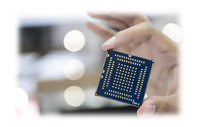
- High-end IC packaging
Application scenarios: FCCSP, SIP modules
Technical advantages: support 0.35MM ultra-thin packaging, suitable for copper pillar bump (CU PILLAR) process
- Storage devices
Typical product: EMMC/UFS memory chip
Key metrics: can carry 8 layers of stacked NAND chips, high temperature characteristics to extend the data retention cycle
- RF front-end module
5G application: PA module packaging
Performance highlights: low dielectric loss reduces signal attenuation (insertion loss <0.5DB/MM), high dimensional stability (warp <0.1%)
- Automotive electronics
Vehicle regulations: AECQ100 certification
Special design: Add ALN filler to improve thermal conductivity (>1W/MK) and resist humidity and heat aging (85℃/85%RH test 1000H)
- Material innovation
High frequency modification: develop low polarity BT resin with DK <3.5
Nano composites: Graphene/BT composites improve thermal conductivity (>5W/MK)
- Process upgrading
Ultra-thin: 25ΜM glass fiber cloth +30ΜM resin layer
3D integration: 3D SIP is achieved in combination with TSV technology
- Emerging applications
CHIPLET Packaging: as an intermediary layer (INTERPOSER) material
Quantum computing: development of extremely low dielectric loss substrates (DF<0.005)
- Sustainable development
Biobased BT resin: using renewable raw materials
Halogen-free flame retardant system: phosphorus and nitrogen synergistic flame retardant technology
BT resin substrate is irreplaceable in the fields of storage, RF and automotive electronics due to its heat resistance, dimensional stability and high frequency performance. In the future, with domestic substitution and technological iteration, BT substrate will be supported by other advanced packaging materials (ABF, glass substrate) to support the high-end demand of the semiconductor industry.


