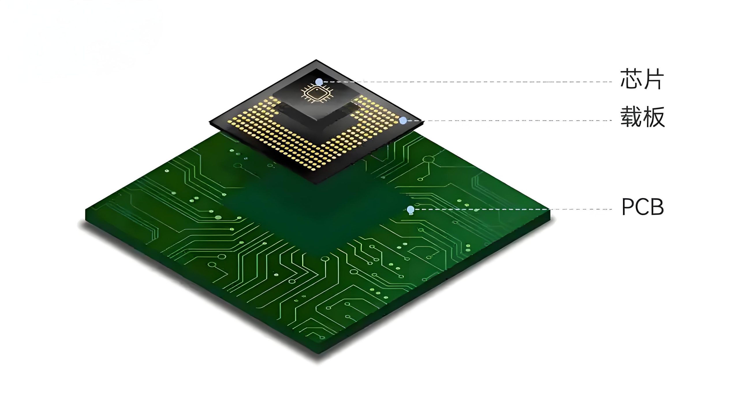
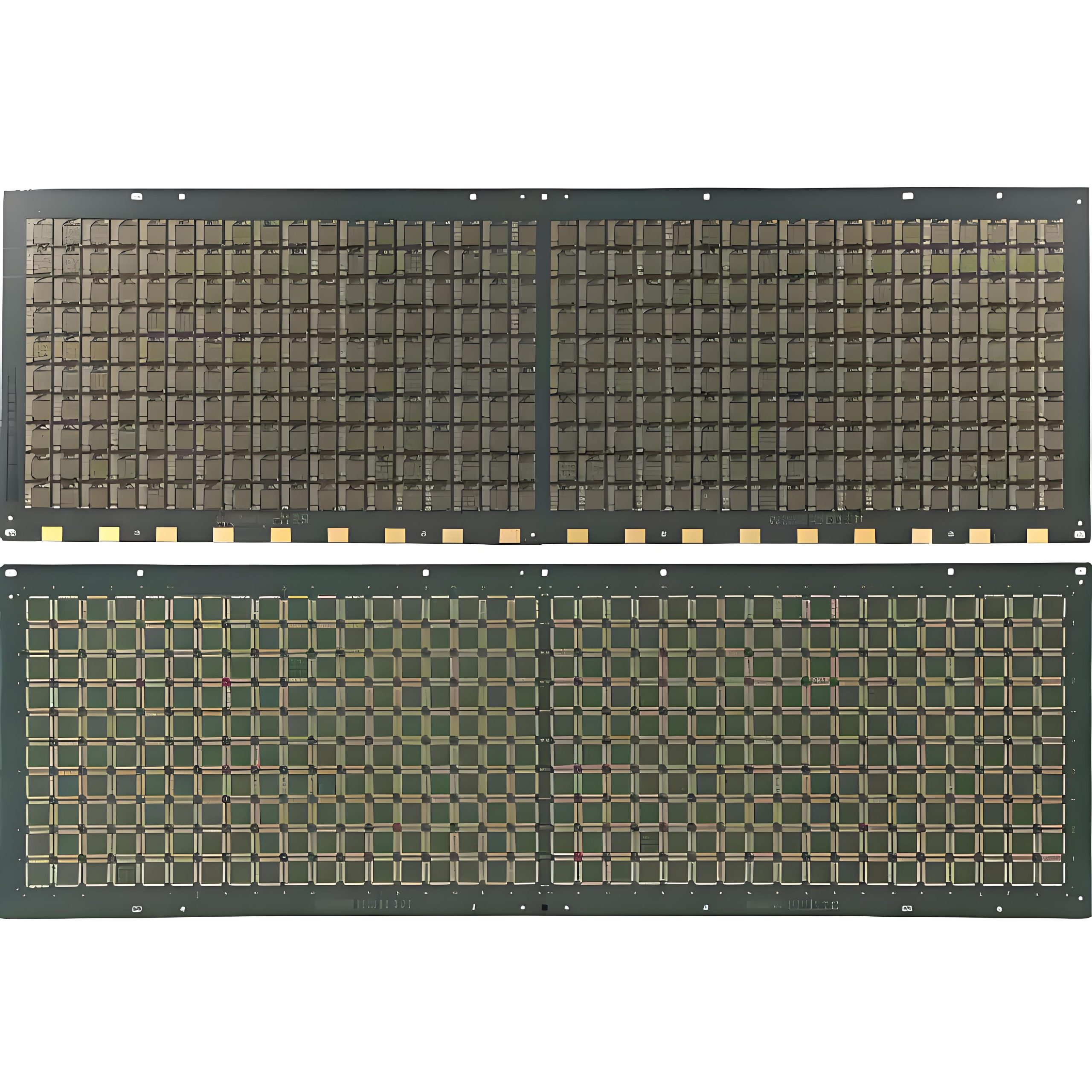
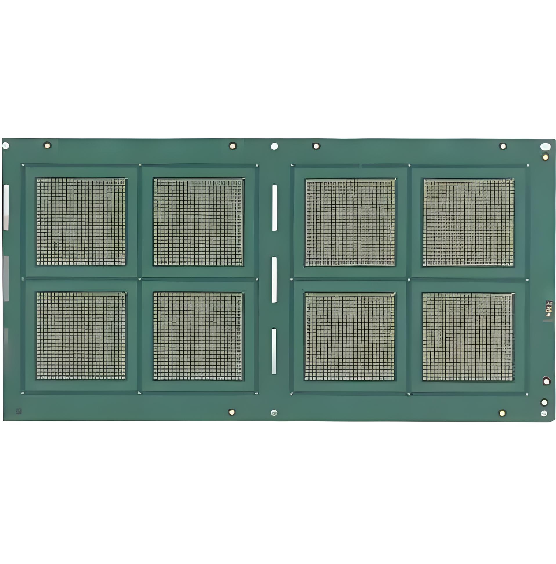
- Ceramic matrix:
insulating course:
Alumina (AL₂O₃): high purity (92%~96%), low cost, dielectric constant 9~10, thermal conductivity (20-30 W/M·K), suitable for basic insulation.
Aluminum nitride (ALN): high thermal conductivity (170~200 W/ (M·K)), low expansion (4.5 x 10⁻⁶/℃), suitable for high power heat dissipation.
Glass ceramics: such as cordierite (2MGO·2AL₂O₃·5SIO₂), with extremely low expansion (<1 x 10⁻⁶/℃), for precision size control.
Function layer:
Silicon nitride (SI₃N₄): high strength (bending strength 700~1500 MPA), corrosion resistant, heat shock resistance, used for high pressure insulation, suitable for extreme environment.
Zirconia (ZRO₂): toughening (fracture toughness 8~12 MPA·M¹/²), high temperature resistance (1600℃), used for structural enhancement.
Low temperature co-fired ceramic (LTCC): glass composite ceramics (such as AL₂O₃+ glass phase), sintering temperature <900°C, can be co-fired with silver/copper conductors.
High temperature co-fired ceramics (HTCC): pure AL₂O₃ or ALN, sintering temperature>1600°C, requires tungsten/molybdenum and other high melting point metal conductors.
- Metal conductor layer
Inner conductor:
Tungsten (W): melting point 3422℃, suitable for high temperature co-firing (HTCC, 1500~1600℃).
Molybdenum manganese (MO-MN): Strong bonding with ceramics, used for airtight packaging.
Outer conductor:
Copper (CU): High conductivity (58 MS/M), high thermal conductivity achieved through DBC (direct bonded copper) technology.
Gold (AU): Antioxidant, used for high frequency signal transmission (such as 5G module).
- Binder and filler
Organic binder: polyvinyl butyral (PVB), used for slurry dispersion in cast film molding.
Inorganic filler: silica (SIO₂) to adjust the sintering shrinkage and reduce interlayer stress.
- Flowing molding (TAPE CASTING):
Ceramic powders (such as AL₂O₃, ALN) are mixed with binders and plasticizers to form slurry (solid content 50%~60%). The slurry is cast by a blade and formed into a film with a thickness of 5~200 ΜM. After drying, the slurry is cut into green pieces.
- Printed circuit:
Print circuit patterns on green sheet with metal paste (such as AG-PD, W), line width precision ≤ 50 ΜM,
- Stacking and pressing:
The multi-layer green sheet is positioned and aligned, and hot pressed (80~150℃,5~20 MPA) to form the green body.
- Co-firing (CO-FIRING):
LTCC: Glass-ceramic systems (such as AL₂O₃-SIO₂-B₂O₃) are sintered at 850~950℃ and compatible with silver conductors
HTCC: Sintered in a hydrogen environment of 1600-1800°C, the high temperature resistance of the metal conductor must be matched.
- Post-treatment:
Surface metallization: sputtering of TI/CU/NI/AU layers to achieve surface packaging pads.
Hole filling: After laser drilling (hole diameter 50~200 ΜM), conductive paste is filled to form vertical interconnection.
Precision machining: diamond grinding wheel, flatness ≤10 ΜM, edge roughness RA<1 ΜM.
- Comparison of material properties
| Material | Thermal conductivity (W/M·K) | Thermal expansion coefficient (PPM/°C) | Mechanical strength | Applicable scenarios
| AL₂O₃ | 20-30 | 6-7 | Medium | Universal, low cost
| ALN | 170-200 | 4.5-5.5 High power, high frequency
| SI₃N₄ | 20-30 | 2.5-3.5 | Extremely high | Heat shock resistance, high reliability
| LTCC | 2-5 | 5-7 | Medium | High frequency, 3d integration
| HTCC | 20-30 | 6-7 High temperature, high density wiring
- Comparison with single-layer ceramic substrate
| Comparison dimension | Single-layer ceramic substrate | Multilayer ceramic substrate
| Functional integration | Single insulation/thermal conductivity Integrated circuit, heat dissipation, shielding, etc
| Interconnection density | Planar wiring | Three-dimensional wiring
| Heat dissipation efficiency | depends on external heat sink | internal thermal layer direct heat dissipation
| reliability | Weld stress concentration | Stress dispersion between layers
| Typical applications | LED packaging, ordinary substrate | 5G module, automotive power control
- Advantages of different material combinations
- Advantages of multi-layer structure:
High density wiring: supports complex three-dimensional circuit design and reduces volume.
Heat management: Rapid heat dissipation through the thermal layer (such as ALN) to improve device life.
Impedance matching: The dielectric constant of LTCC is adjustable (5-10), suitable for high frequency signal transmission.
- Material selection advantages:
ALN: used for IGBT and laser diode to solve the problem of high power heat dissipation.
LTCC: integrated passive components (capacitors, inductors), suitable for 5G millimeter wave antennas.
SI₃N₄: Automotive electronics with vibration and high temperature (>300°C) resistance.
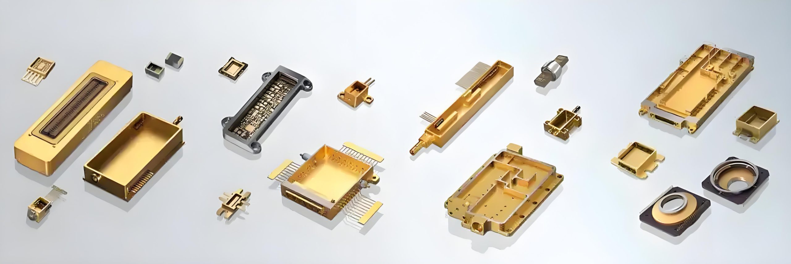
- Industry application and technical index advantages
- Semiconductor power module:
The voltage is greater than 3 KV and the heat conduction is greater than 150 W/M·K. It can be used as an inverter for electric vehicles
- High frequency communication (5G/6G):
Dielectric loss <0.002 (@10 GHZ), high signal integrity, used in base station RF front end (LTCC filter, antenna).
- Aerospace and military industry:
Radiation resistant and extreme temperature resistant (-55°C to 300°C), used in satellite power system, radar T/R components.
- Medical electronics:
Biocompatibility, high reliability (MTBF> 100,000 hours), implantable devices.
- Detection sensor
Temperature range-200℃~800℃, moisture resistant (moisture absorption rate <0.1%), suitable for deep sea detector
- Industries particularly suitable
- High power electronic devices
IGBT module: multi-layer ALN/AL₂O₃ substrate reduces junction temperature and increases power density to 150 W/CM².
Laser diode array: low thermal resistance design (<1℃/W) to ensure beam stability.
- Communications
5G RF module: LTCC supports 28 GHZ millimeter wave band and reduces the size by 50%.
Optical module: multi-layer structure to achieve optical-electrical hybrid packaging, transmission rate up to 100 GBPS.
- Automotive electronics
Power lithium battery BMS: high temperature resistant (125℃), anti-vibration, to ensure the safety monitoring of battery pack.
Lidar (LIDAR): High density interconnect supports more than 128 channels of laser transmission/reception.
The ALN substrate is used for motor controller, and the heat dissipation efficiency is 5 times higher than that of AL₂O₃.
- Aerospace
Satellite payload circuit: radiation resistant (total dose 10⁶ RAD), lightweight, suitable for deep space exploration.
Rocket engine controller: resistant to extreme temperature cycles (-196℃~300℃).
- Medical equipment
MRI gradient coil: high insulation (> 10¹⁴ Ω · CM) to avoid electromagnetic interference.
Implantable neural stimulator: airtight packaging (leakage rate <1 x 10⁻¹⁰ PA · M³/S) to prevent body fluid invasion
- Nanostructured ceramic layer: such as AL₂O₃ nanowires to enhance the interfacial bonding force;
- Co-packaging of heterogeneous materials: 3D integration of ceramic-silicon-metal;
- Intelligent manufacturing: AI optimizes sintering process parameters and reduces defect rate.
In the fields of new energy vehicles, 6G communications and quantum computing, multilayer ceramic substrates will continue to play the role of “bones of electronic systems”
sum up
Multilayer ceramic substrates, through the synergistic optimization of materials and processes, far surpass traditional PCBs or metal substrates in terms of power density, high-frequency performance, and reliability. In the future, with the widespread adoption of wide bandgap semiconductors (SIC, GAN), the demand for high thermal conductivity and high-temperature resistant ceramic substrates will continue to grow, especially in the fields of new energy, communications, and aerospace.


