In today’s digital economy, the backbone of data centers and long-haul networks is no longer built on copper. Fiber and advanced optical chips drive massive streams of information that power cloud computing, AI workloads, and international communication. Yet fiber alone is not enough; it must work with chips that handle light precisely, using high-frequency materials and efficient packaging. This is where companies like DEEPETCH step in. With a portfolio that ranges from IDM-based semiconductor integration to stocked chips for immediate deployment, the company has built a reputation for bringing precision materials into real-world communication networks.
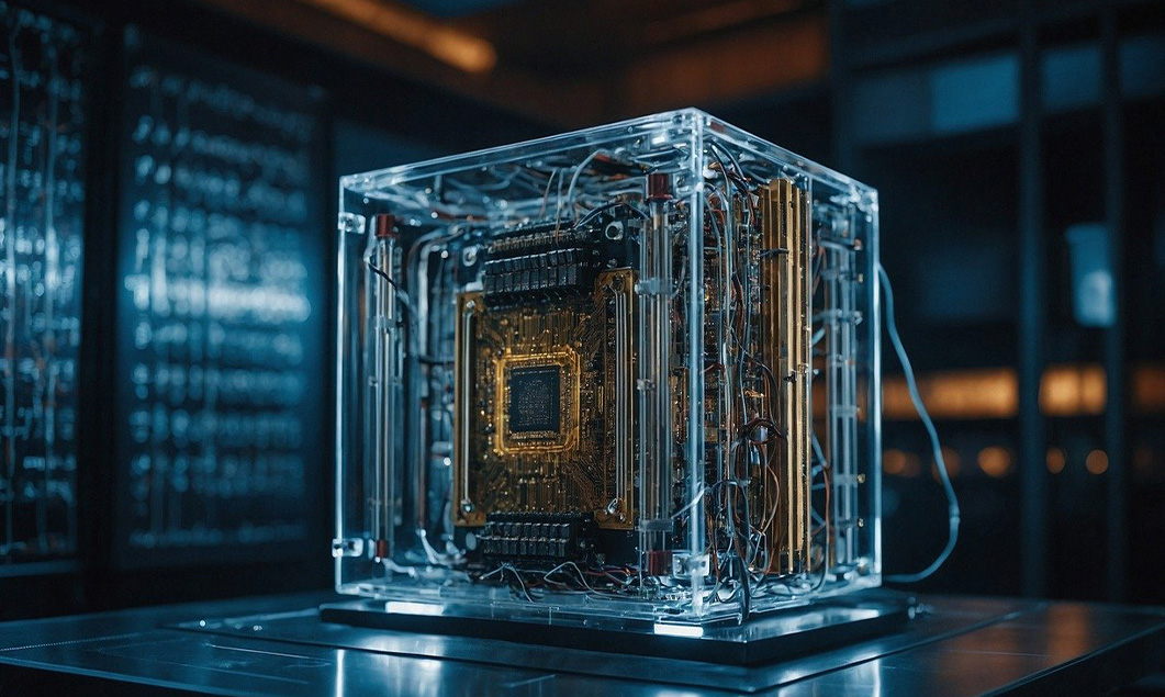
Optical chips may look small, yet in practice they hold the key to stable signal delivery. In high-density racks, each chip converts and routes or modulates optical signals that carry data, working with modules and electronic switches to direct the flow of information. A flawed chip design or poor-quality substrate can introduce loss, jitter, or downtime. When combined with transceivers and optical modules made from advanced semiconductors, these chips become more than components. They form the core engine that keeps your system running as promised.
Signal transmission depends on converting and routing light with minimal noise. Modern chips are designed to handle high bandwidth with minimal optical loss, allowing you to maintain integrity across long distances. Pairing them with InP-based detectors can reduce noise, as these devices achieve quantum efficiencies above 90% at the 1550 nm band.
Every growing data center faces the same problem: how to add capacity without tearing down existing systems. Optical chips provide the flexibility to scale by supporting new modulation formats or higher baud rates. You can shift from 400G to 800G deployments by using chips that support faster symbol rates.
Chips are also about predictable behavior. In practice, they are packaged into optical modules or subsystems. If one module shows degradation, it can be swapped out without shutting down the whole network. This modular design reduces downtime and supports planned maintenance cycles, which most operators value more than peak speed.
As speeds climb, the role of chips becomes even sharper. A single mismatch in bandwidth can negate the benefits of high-end modules. That is why the relationship between chips, transceivers, and substrates matters.
High-capacity data centers now adopt 800G and even 1.6T modules. Optical chips must align with these transceivers, handling both the throughput and the thermal load. Without advanced chips, those modules cannot perform as intended.
The backbone of many optical modules today is InP. With a direct band gap aligned to 1550 nm and strong radiation resistance, InP is widely used in optical modules despite having lower electron mobility than GaAs.
Optical chips with precise fabrication and core alignment keep insertion loss minimal. For high-frequency applications, even a fraction of a decibel matters. In practical terms, this can be the difference between meeting a service level agreement and failing it.
Reliable systems rely on materials and modules that match the speed of the network. Some companies provide cables, some provide chips, but integrated suppliers can offer chips, substrates, and packaging.
InP has better thermal conductivity than gallium arsenide, around 68 W/m·K at room temperature. This makes it fit for high power density devices like backbone lasers. Using such substrates reduces heat stress and keeps your system more stable under heavy loads.
From 400G up to 1.6T, modules are available that match current data center roadmaps. Each is designed to work with standard optical chips, reducing complexity during upgrades.
Not every environment is the same. Whether it’s a hyperscale center or a telecom edge node, chips can be tailored in wavelength range, detector type, and package style to match the setup.
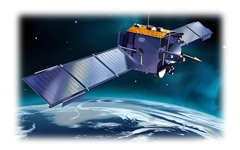
Communication Industry covers more than one use case. It stretches from data centers to 5G towers to satellites. Products based on InP and optical chips can cross all these areas.
In large halls packed with servers, bandwidth demand doubles almost yearly. Modules and chips designed for multi-terabit throughput keep that growth manageable.
Base stations rely on low-loss transmission for fronthaul and backhaul. InP-based lasers and detectors support the 1550 nm band, which is the sweet spot for low-loss fiber transmission.
Radiation resistance is another angle. InP tolerates high radiation levels and works across −200 °C to +300 °C. When combined with robust packaging, this makes it suitable for aerospace payloads.
At the core of these solutions lies the choice of semiconductor. The decision matters because it defines efficiency, stability, and long-term costs.
InP-based devices have been demonstrated in sub-THz imaging and communication, typically in the 0.3–1 THz range, with research pushing further. For next-generation applications like ultra-fast wireless or high-resolution imaging, this property makes it future-proof.
With a direct band gap of 1.35 eV, InP aligns perfectly with 1550 nm, the lowest loss point of optical fiber. This is why it’s called the “core material” of the communication backbone.
Environments like satellites or deep-space sensors need devices that still work under radiation and temperature extremes. InP delivers here, while silicon struggles.
Technology never stops. Even if today’s systems feel fast, tomorrow’s requirements will demand more.
Moving from 800G to 1.6T is just the beginning. Researchers are already aiming at multi-terabit links, which will put even more stress on chips and modules.
Future InP devices may support quantum communication through single photon sources. Optical chips will then play roles in processing these ultra-sensitive signals.
Mass production alone is not enough. Facilities must now provide traceability, simulation, and predictive maintenance. This also extends to custom optical chips, which are made to meet each network’s unique profile.
Q1: Why is Indium Phosphide important in optical communication?
A: It aligns with the 1550 nm low-loss window, has good thermal conductivity, strong radiation resistance, and operates across extreme conditions.
Q2: Can optical chips affect the performance of high-speed modules?
A: Yes, poor-quality chips can increase loss and negate the benefits of advanced transceivers.
Q3: Are optical chips customizable for different needs?
A: Yes, they can be designed for different wavelengths, speeds, and packaging styles.

The DE-CW-1310 DFB EPI wafer, a high-performance epitaxial structure designed for distributed feedback (DFB) lasers operating at 1310 nm....

Ceramic thin-filmvacuum sensor Optical gas massflowmeter Liquid mass flowmeter Force sensor MEMS...

Photoelectric sensing chip Light source chips Optical transmission and modulationchips Optical detection and receptionchips...

Using a“Detach Core”which has two-layers carrier foil structure on the surface as a core, and forming...

Tenting process is a kind of subtractive process, the process as follows: Laminating photosensitive film...

Modified Semi-Added Process abbreviated as mSAP, which can be used on the core or build-up layers, pattern...

Semi-Added Process abbreviated as SAP, using on the build-up-layer pattern forming as follow:First depositing...

The product generally adopts the pressing lamination process of semi-curing sheets , and line formation...

The products generally adopt the Build-up Film Lamination process, and the circuit formation uses the...

Equipment features: 1. Non-destructive precision testing Micrometer-level probe contact technology...