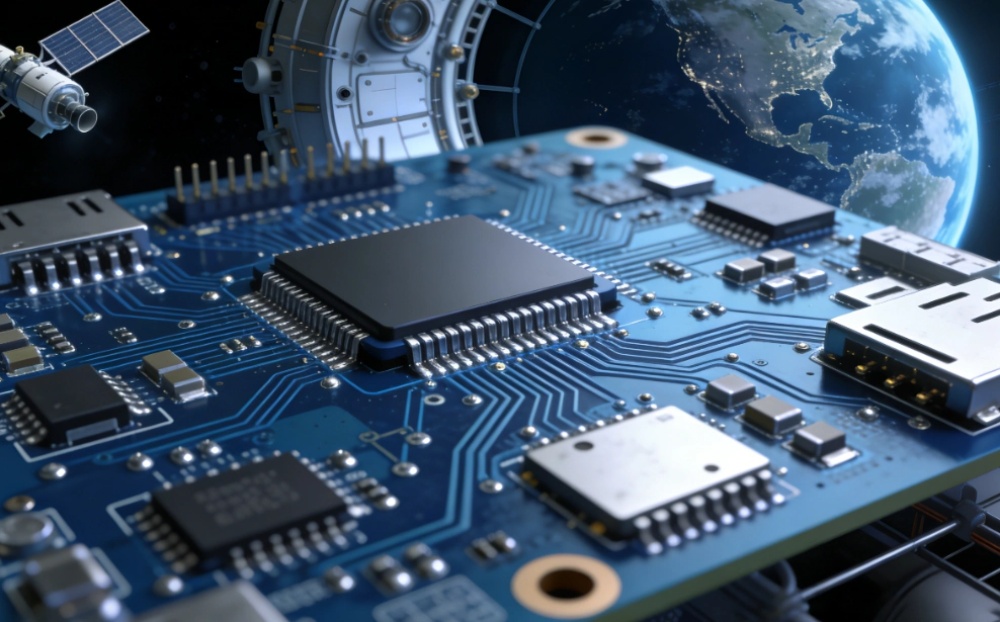
Creating electronics for space ranks among the toughest tasks in current engineering. A minor issue, such as a faulty solder connection, could endanger an entire costly mission worth millions. You face a vacuum environment that draws moisture from substances. Radiation can alter data in logic components unexpectedly. Following strict reliability standards ensures your equipment withstands space vacuum, sharp temperature changes, and intense radiation exposure. This overview covers five key guidelines, from selecting superior substrates to using custom enclosures, and explains how expert production connects lab models to actual space use.
Space vacuum eliminates air-based heat transfer through convection. Therefore, heat removal depends solely on conduction across the board and emission from outer layers. Without precise thermal planning, parts will hit critical temperatures quickly, leading to operational breakdowns. Engineers should view the board as a heat conduit rather than just a wiring platform.
Materials such as ceramics or metal cores aid in shifting heat from energy-intensive parts. The selection of these base elements determines the durability of the full satellite setup. Proper choices extend operational life significantly. Thus, they support reliable performance over time.
In orbital AI processing units, basic passive methods fall short. Adding liquid cooling into the design enables managing high heat loads from 400G or 800G optical systems. This prevents speed reductions during heavy use. As a result, it maintains steady output in demanding conditions.
As a PCBA experiences shifts from -150°C to +150°C while passing through Earth’s shadow, substances expand and shrink at varying speeds. Matching the Coefficient of Thermal Expansion (CTE) between components and the base avoids strain on solder points. Such alignment reduces wear over repeated cycles. Consequently, it enhances long-term stability.
Deep space contains heavy ionizing radiation that triggers Single Event Effects (SEE). This resembles an unseen force randomly altering processor functions. To preserve data accuracy, combine hardware protections with effective barriers. These measures safeguard against environmental threats.
Regular silicon risks latching under radiation exposure. Employing Silicon On Insulators (SOI) technology introduces an oxide barrier that separates transistors. This isolation cuts down on radiation-caused faults and current leaks substantially. Therefore, it boosts overall circuit safety.

Circuit arrangements go beyond base layers to include backup paths. Techniques like TMR (Triple Modular Redundancy) and error detection codes provide essential safeguards. Systems designed this way anticipate radiation impacts and recover from them. As such, they ensure continuous functionality.
Space generates significant electromagnetic noise. Effective barriers extend past simple metal covers on chips. They involve detailed thin-film layers of conductive elements to form protective enclosures without excess mass for launch. This approach maintains signal clarity while keeping weight low.
Rocket liftoff applies strong forces and irregular shakes that could damage typical consumer boards. Standards focus on avoiding tiny breaks in metal paths and layer separations. The journey proves harsh, so boards require robust construction to endure it.
For dependable chips, Ceramic Leadless Chip Carrier Housing (CLCC) sets the benchmark. Ceramic construction offers strong sealing and firmness, shielding inner silicon from launch shocks. This protection preserves component integrity during intense motion. Thus, it supports mission success.
Placing epoxy resin beneath large BGA parts spreads stress evenly across the unit. This prevents concentration on small solder spheres. Such a process, though straightforward, protects against failures in key areas. Consequently, it contributes to overall structural strength.
In tight spaces, a FCCSP Substrate delivers a compact, lightweight option over traditional forms. These bases align with existing frameworks while providing resistance to bending under temperature variations. Their design ensures compatibility and durability. As a result, they fit well in constrained setups.
Satellite and radar operations demand accurate high-frequency handling with no tolerance for mistakes. If TR (Transmit/Receive) units fail to manage gigahertz bands with low signal drop, links will fail. Combining advanced EMS with semiconductor expertise proves crucial here.
From my experience in the sector, numerous initiatives stumble by overlooking supply details. DEEPETCH excels through its full IDM (Integrated Device Manufacturing) approach. They manage from design to custom enclosures, not just assembly. For TR transceiver needs or quick access to chips in stock, their emphasis on fields like aerospace and 6G positions them as a true ally for vital operations.
Building TR modules calls for exact wire connections and chip flipping methods. Maintaining signal quality at fine scales ensures smooth shifts between transmission and reception without disruptions. These techniques preserve data flow integrity. Therefore, they enable reliable communication.
Minimizing signal reduction remains critical. Low-loss insulators and accurate resistance management on board paths amplify faint space signals properly. This avoids blending them into background interference. As such, it secures clear transmissions.
Current radar setups need dense power handling. Incorporating GaN (Gallium Nitride) or GaAs (Gallium Arsenide) elements into EMS processes demands unique tools and checks beyond typical factories. Specialized equipment ensures proper integration. Consequently, it meets performance requirements.
Vacuum conditions cause common materials like plastics and glues to emit trapped vapors, known as outgassing. These vapors settle on optics or detectors, impairing satellite functions. Adopting a no-leakage mindset for all board materials becomes essential.
Solder covers, glues, and protective layers require NASA or ESA approval for minimal emissions. The added expense proves worthwhile compared to impaired viewing devices. Certified options prevent such issues effectively. Thus, they safeguard mission objectives.
For vacuum-exposed parts, sealed ceramic or metal enclosures provide protection. They create a small inert gas area around chips, replicating ground conditions in space. This method sustains normal operations amid emptiness. As a result, it enhances reliability.
Space production demands controlled environments like Class 100 cleanrooms. This prevents dirt particles from embedding under layers, which might lead to emissions or shorts later. Strict protocols maintain purity throughout. Therefore, they support flawless assembly.
Q1: Why is Silicon On Insulator (SOI) preferred over standard silicon for space?
A: Standard silicon is vulnerable to radiation latch-up, which can permanently damage a chip. SOI provides a physical insulation layer that blocks these parasitic currents, making the hardware much more resilient to cosmic rays.
Q2: What is the biggest risk of using consumer-grade PCBAs in a satellite?
A: Outgassing is a silent killer. Standard FR4 boards and cheap plastics release vapors in a vacuum that coat sensors and lenses, potentially ruining the mission’s primary scientific or communication goals.
Q3: How does DEEPETCH handle the current global chip shortage for aerospace?
A: By maintaining an extensive inventory of chips in stock and utilizing an IDM model, they can bypass many of the supply chain bottlenecks that delay traditional “design-then-outsource” projects.
Q4: Can I use standard soldering techniques for space-grade boards?
A: Not exactly. Space-grade soldering requires specific alloys and much stricter inspection standards (like IPC Class 3) to ensure joints don’t develop “tin whiskers” or cracks under extreme thermal cycling.
Q5: What makes a TR transceiver module “space-ready”?
A: It must combine high-frequency performance with extreme thermal management and radiation hardening. It’s not just about the circuit; it’s about the ceramic packaging and the ability to dissipate heat without air.

The DE-CW-1310 DFB EPI wafer, a high-performance epitaxial structure designed for distributed feedback (DFB) lasers operating at 1310 nm....

Ceramic thin-filmvacuum sensor Optical gas massflowmeter Liquid mass flowmeter Force sensor MEMS...

Photoelectric sensing chip Light source chips Optical transmission and modulationchips Optical detection and receptionchips...

Using a“Detach Core”which has two-layers carrier foil structure on the surface as a core, and forming...

Tenting process is a kind of subtractive process, the process as follows: Laminating photosensitive film...

Modified Semi-Added Process abbreviated as mSAP, which can be used on the core or build-up layers, pattern...

Semi-Added Process abbreviated as SAP, using on the build-up-layer pattern forming as follow:First depositing...

The product generally adopts the pressing lamination process of semi-curing sheets , and line formation...

The products generally adopt the Build-up Film Lamination process, and the circuit formation uses the...

Equipment features: 1. Non-destructive precision testing Micrometer-level probe contact technology...