Many new industries are growing fast today because of special materials. These include 5G networks, Electric Vehicles (EVs), and smart Internet of Things (IoT) gadgets. At the heart of this big change are Compound Semiconductor Wafers. These wafers, like Gallium Arsenide (GaAs), Silicon Carbide (SiC), Indium Phosphide (InP), and Gallium Nitride (GaN), work much better than standard silicon. They offer high speed, handle more power, and remain stable when temperatures rise. Yet, these unique traits create a major issue in manufacturing: moving these fragile, costly materials safely. Simple silicon wafer carriers are simply not good enough. The true answer lies in custom carrier trays. These trays are carefully made to protect your valuable substrates all through the complex manufacturing journey.
You need more than just a parts supplier; you need a partner with deep material knowledge. This is where DEEPETCH truly shines. DEEPETCH is an Integrated Design and Manufacturing (IDM) company. They supply advanced materials like Gallium Arsenide (essential for super-fast circuits) and Silicon Carbide (the key material for powerful high-power electronics). DEEPETCH uses this deep material understanding to fix difficult process problems, such as wafer handling. Their skill set covers MEMS and advanced packaging. This ensures every custom carrier tray they help design is a perfect match for your wafer and your specific process needs.
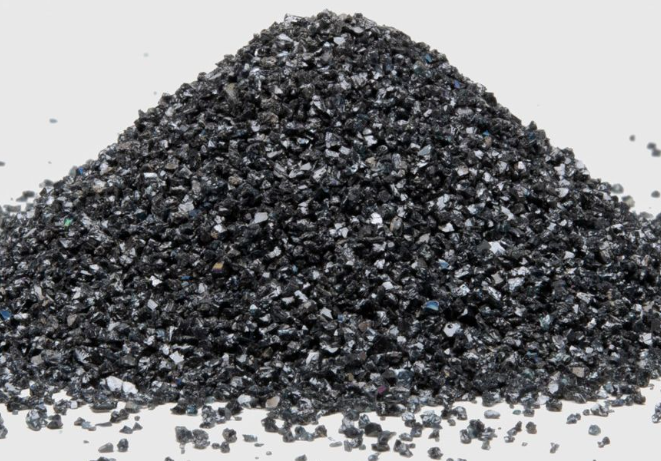
Compound semiconductor wafers are entirely different from standard silicon. They are easily harmed by pressure, heat, and dirt. III-V Wafers (GaAs, InP) are naturally breakable. They risk costly cracks when machines handle them. SiC and GaN often need manufacturing steps at very high temperatures, sometimes exceeding 1600°C. Simple plastic carriers cannot survive this heat. All these materials are also very sensitive to Metallic Contamination or tiny particles. This dirt can severely damage the electronic and light performance of the finished chip. Carriers must address these three main risks.
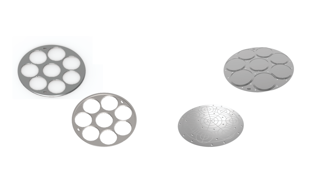
The manufacturing of customized wafer carrier trays, from initial concept to final delivery, is a rigorous and systematic process. The entire procedure is divided into four key steps, ensuring the tray perfectly matches the demanding requirements of compound semiconductors, thereby achieving ultimate protection for high-value wafers. These four core stages cover comprehensive considerations from requirement definition, material selection, structural design, to quality verification.
Custom design starts by matching the tray to your specific factory environment. Wafers often come in non-standard sizes (e.g., 100mm, 150mm for Indium Phosphide) and are made very thin. The carrier must provide great support to prevent warping. It must also survive process limits like strong chemicals or high vacuum. Finally, your custom carriers must fit exactly with all Automation Equipment (robotic arms) to ensure smooth, damage-free wafer movement.
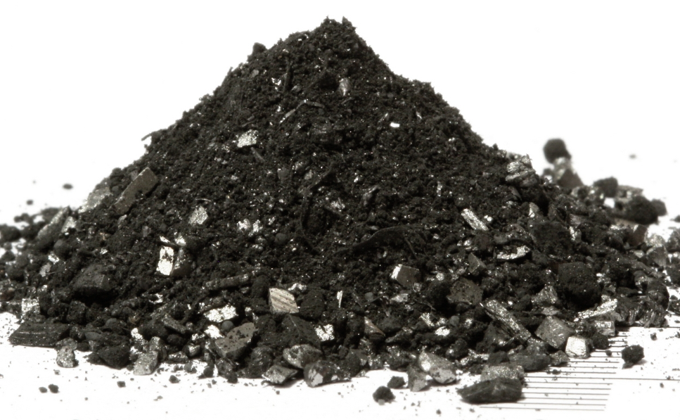
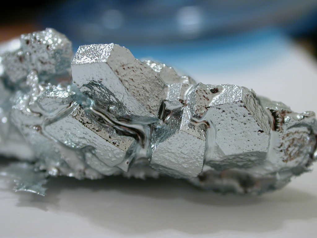
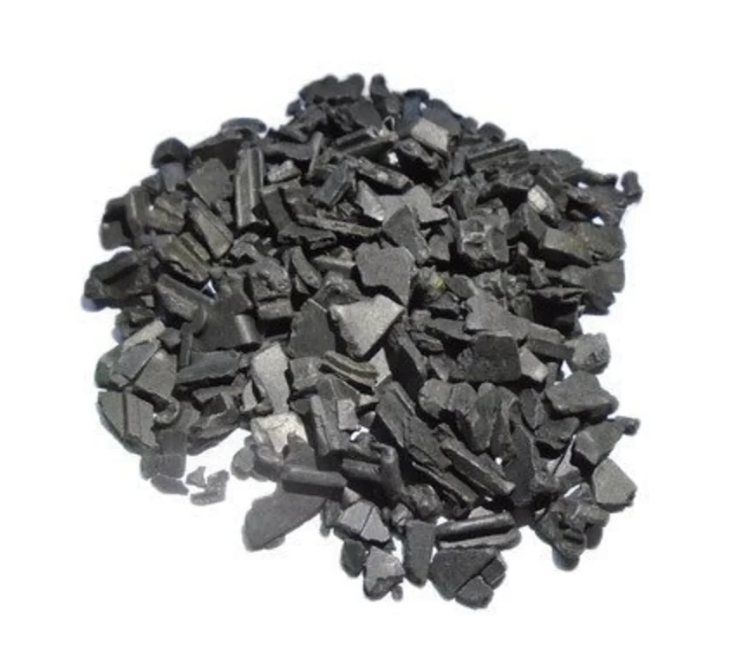
Picking the right material fixes problems related to contamination and heat. For chemical processes using liquids, use High-Purity Plastics like PEEK or PTFE. They resist chemicals and shed minimal particles, stopping metal ion contamination. For static electricity protection, materials need Static Dissipative features (e.g., special polymers) to safely drain static charges away. For extreme heat processes (often reaching over 1800°C) found with SiC and Gallium Nitride, use stable materials like Quartz or ultra-high-purity Graphite.
The wafer’s surface is the active area, so the carrier must touch it as little as possible. Edge-Grip designs, such as precision V-grooves, hold the wafer only at its bevel. This minimizes contact points, reducing the chance of micro-scratches. For advanced wafers processed on both sides, Unique Pocket Geometry is required. This shape provides support only at the very edge. Finally, Stress Reduction Features (like gentle, rounded corners and smart vents) are vital to ensure ultra-thin substrates stay flat and stress-free during processing.
A perfect design can still fail without strict factory standards. You must check that the manufacturer follows strict Quality Management Systems like ISO 9001 to guarantee material purity. Every finished carrier must undergo Rigorous Cleaning in a certified cleanroom to remove all particles and residue. Detailed Traceability records must be kept for every batch, detailing materials and cleaning logs, allowing for quick problem-solving if dirt is found.
The pursuit of the perfect carrier demands expertise across the entire semiconductor supply chain, moving far beyond simple mechanical engineering. Working with a company like DEEPETCH provides immediate access to a wealth of integrated knowledge, essential for tackling the unique complexities of compound materials.
DEEPETCH’s foundation as a supplier of advanced substrates—including GaAs, SiC, InP, and GaN—means their engineers naturally understand the critical characteristics of these wafers.
By adopting the IDM Model, DEEPETCH controls the entire lifecycle, from initial concept and engineering specifications to final production and quality control. This integrated approach is crucial for highly specialized components like custom carriers. It seamlessly links material science (wafer/carrier materials) with physical handling design, providing the client with a single source of accountability. This significantly reduces compatibility issues often encountered when using separate design and manufacturing firms.
The advantage extends to the final product stage. DEEPETCH’s deep experience in MEMS chips and power semiconductors ensures the carrier design anticipates downstream complexities. For example, they account for the special support required for ultra-thin wafers (used in MEMS) during thinning processes, or the high thermal stability needed for SiC power device annealing, ensuring the carrier provides perfect support during the wafer’s most vulnerable post-processing stages.
Q1: Why can’t I just line a silicon carrier with a soft material for GaAs wafers?
A: Lining creates contamination risks from the material shedding and glue outgassing. Custom carriers use precision-machined, single-piece, high-purity materials to eliminate these risks.
Q2: What specific design feature protects ultra-thin wafers from warping?
A: Stress Reduction Features, which include gentle radius fillets and smart vents, are used to equalize pressure and prevent excessive force across the thin surface.
Q3: Is ESD protection necessary for all compound semiconductor carriers?
A: Yes. Static discharge can instantly and permanently damage sensitive devices (MMICs/sensors) built on these wafers, necessitating static dissipative carrier materials.

The DE-CW-1310 DFB EPI wafer, a high-performance epitaxial structure designed for distributed feedback (DFB) lasers operating at 1310 nm....

Ceramic thin-filmvacuum sensor Optical gas massflowmeter Liquid mass flowmeter Force sensor MEMS...

Photoelectric sensing chip Light source chips Optical transmission and modulationchips Optical detection and receptionchips...

Using a“Detach Core”which has two-layers carrier foil structure on the surface as a core, and forming...

Tenting process is a kind of subtractive process, the process as follows: Laminating photosensitive film...

Modified Semi-Added Process abbreviated as mSAP, which can be used on the core or build-up layers, pattern...

Semi-Added Process abbreviated as SAP, using on the build-up-layer pattern forming as follow:First depositing...

The product generally adopts the pressing lamination process of semi-curing sheets , and line formation...

The products generally adopt the Build-up Film Lamination process, and the circuit formation uses the...

Equipment features: 1. Non-destructive precision testing Micrometer-level probe contact technology...