The transition from 5G to 6G involves more than quicker movie downloads. It ushers in a period of Integrated Sensing and Communication (ISAC). As a result, hardware must manage sensing, computing, and intelligence simultaneously. Professionals in the electronics industry encounter significant challenges with conventional manufacturing approaches. Traditional methods for placing components on boards prove inadequate for Terahertz frequencies. They also fall short of the rigorous precision essential for 2026 hardware.
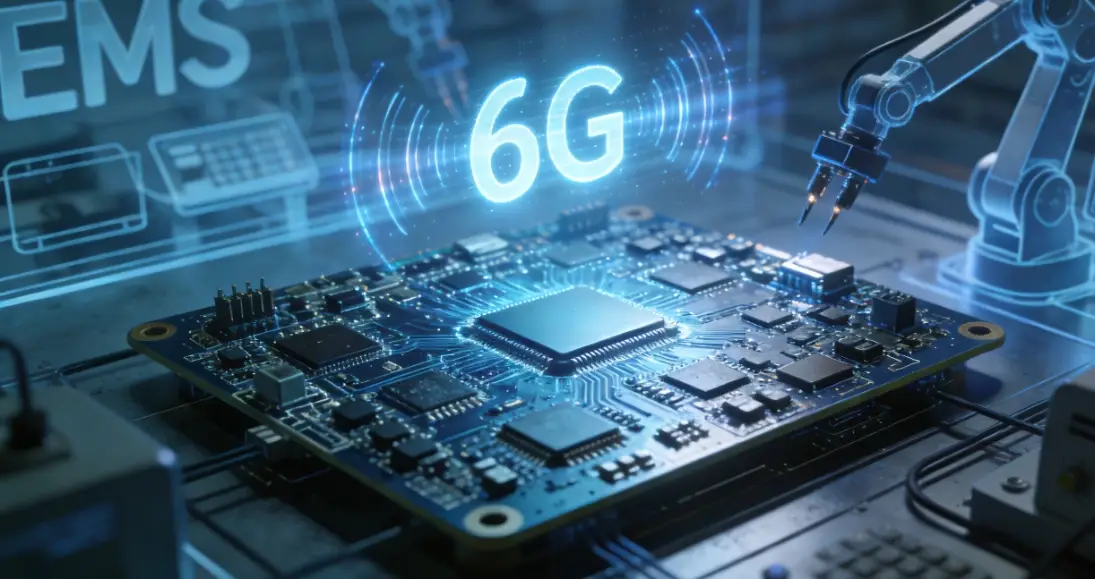
The year 2026 establishes a clear boundary for electronic manufacturing services. Industry specialists observe a substantial shift toward tailored EMS solutions that exceed basic assembly. Clients no longer acquire merely a board. Rather, they secure an intricate system capable of perceiving and reasoning.
In the 6G environment, base stations function as expansive radars while processing data concurrently. This sensing aspect introduces additional layers of intricacy to PCBA design, which many conventional facilities have yet to prepare for adequately. Consequently, engineers must address signal isolation through techniques that proved unnecessary five years earlier. Such measures ensure effective separation and maintain operational efficiency.
Signals at high frequencies exhibit considerable sensitivity. Even a minor impedance discrepancy or inadequate soldering can compromise the complete connection. Expertise in semiconductor physics becomes crucial in this context. DEEPETCH excels because it transcends mere assembly; it oversees processes from the wafer stage onward. Founded in 2019, the company has expanded 400G and 800G optical modules and now advances into 1.6T domains. Collaboration with them provides access to an IDM model, where design, manufacturing, and packaging occur under unified management. This approach offers greater reliability for 6G initiatives compared to coordinating among multiple vendors, who may blame one another during setbacks. Ultimately, it streamlines accountability and enhances overall project outcomes.
By emphasizing advanced Aerospace standards, the transition to specialized EMS directly addresses the market’s demand for dependability. Whether for satellite connections or 6G components, production must achieve perfection. These standards foster robust performance in demanding applications.
Constructing a skyscraper on unstable ground proves impossible. Likewise, developing a 6G transceiver on inferior substrates leads to failure. The efficacy of the final product links closely to material science at the supply chain’s outset.
Silicon suits ordinary processors effectively. However, for rapid 6G connections, materials such as Gallium Arsenide (GaAs) emerge as superior choices. GaAs demonstrates electron mobility around 8500 cm²/(V*s), enabling signals to propagate swiftly in contrast to the more leisurely rate of conventional silicon. This characteristic minimizes losses and optimizes transmission in elevated-speed networks.
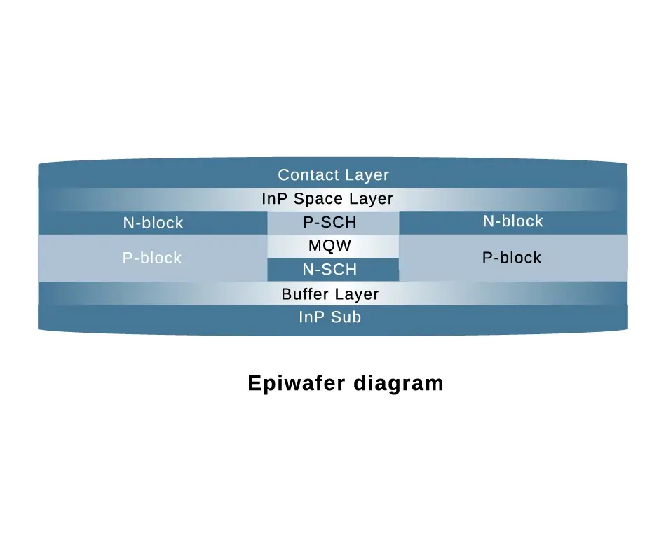
For wavelength consistency in optical links, the DE-CW-1310 DFB Epi Wafer serves as the essential element. It supplies accurate epitaxial layers required for Distributed Feedback lasers, which constitute the core of 100G to 800G transceivers. These layers support stable optical performance and integrate seamlessly into broader communication infrastructures.
Advanced thin-film deposition techniques allow manufacturers to regulate layers at the atomic scale. This level of precision facilitates the development of MEMS and high-frequency sensors. Such sensors achieve compact dimensions suitable for contemporary drones while delivering sufficient potency for 6G requirements. Consequently, they enable innovative applications in compact, high-performance devices.
The space domain presents formidable difficulties for electronic systems. It involves drastic temperature variations, radiation exposure, and no opportunity for repairs upon failure. 6G satellite communications extend these aerospace hurdles to commercial contexts.
Satellite circuits must accommodate millimeter-wave and Terahertz frequencies. At these ranges, the PCBA’s physical configuration integrates directly into the electrical pathway. Thus, every trace dimension and via placement holds critical importance. Designers prioritize meticulous layouts to preserve signal clarity amid orbital conditions.
Transmitter/Receiver (TR) chips function as primary components in these setups. They require high gain and minimal noise, alongside resilience to orbital radiation. The objective remains maintaining signal stability despite environmental threats to the equipment. This durability ensures reliable data transmission in extraterrestrial environments.
“System-in-Package” (SiP) proficiency proves essential when progressing from chips to TR Transceiver Modules. The process focuses on integrating greater functionality within reduced spaces, while preventing excessive heat buildup. These strategies enhance density and thermal regulation for sustained operations.
Designing for UAVs or satellites tolerates no mediocrity, as it invites potential catastrophe. 2026 guidelines mandate an absolute intolerance for production flaws.
Aerospace-grade PCBA incorporates high-TG materials and refined soldering methods to avert fractures from thermal expansion. This resembles fortifying a vehicle for traversal through volcanic terrain—costly yet indispensable. Such reinforcements guarantee endurance and compliance with stringent safety criteria.
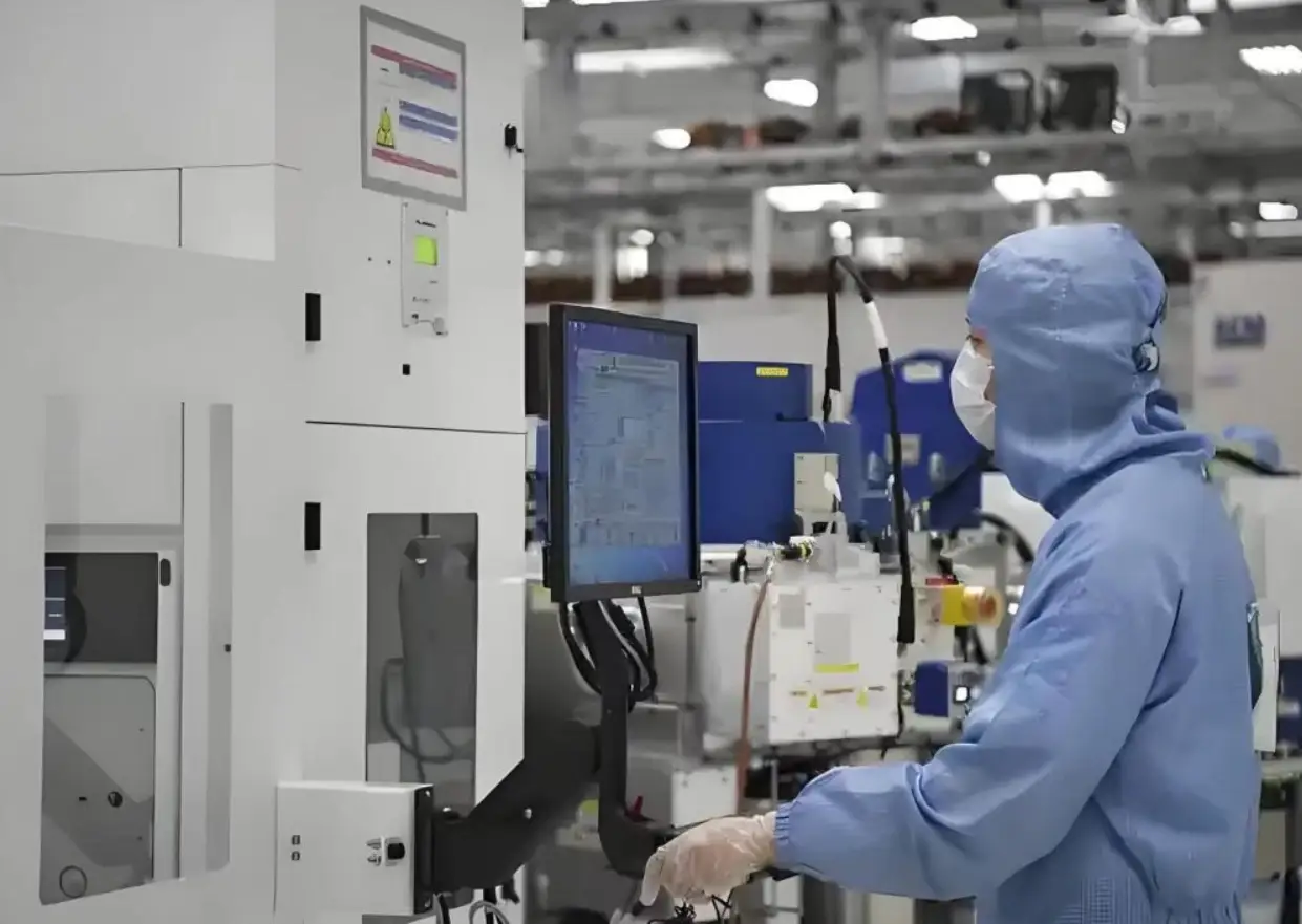
Selecting an EMS provider versed in Company Overview standards such as IATF 16949 or ISO 9001 forms the foundation. Expertise in high-reliability settings, where signal integrity bears life-or-death implications, becomes paramount. Providers with this background deliver comprehensive support and adhere to protocols for superior results.
Each board undergoes intensive thermal cycling and vibration assessments. Should failure occur, it must manifest in laboratory conditions rather than at 500 miles altitude. This rigorous evaluation confirms robustness for critical deployments distant from Earth.
The intelligence facet of 6G necessitates hardware to analyze data at its collection point. This development promotes Edge AI integration within the circuitry itself.
6G devices leverage on-site computing resources instead of transmitting all data to remote clouds. This configuration diminishes latency, proving vital for autonomous drones requiring instantaneous decisions. As a result, it facilitates responsive operations in dynamic scenarios.
Hardware now intertwines with its accompanying software. Within TR modules, firmware frequently offsets hardware constraints, such as thermal variations. This interplay represents the essential foundation of contemporary electronics. It yields optimized systems that harmonize physical and digital elements effectively.
The central processing unit of a drone oversees flight regulation, visual inputs, and 6G telemetry concurrently. A stratified PCBA architecture balances rapid data flows with energy-intensive propulsion systems. This equilibrium supports seamless functionality in aerial missions.
Markets advance rapidly, yet global supply chains remain somewhat disorganized. Achievement in 2026 hinges on access to components and the capability to assemble them proficiently.
Extended delays for particular components pose major obstacles. Partnering with suppliers maintaining Chips in Stock prevents project halts entirely. This oversight detail frequently escapes attention until crises arise. It sustains momentum and averts disruptions in development timelines.
Numerous firms excel at crafting a single exemplary prototype in controlled settings. The genuine challenge lies in producing 10,000 units with consistent quality. Reliable EMS collaborators span this divide by resolving manufacturing issues promptly. Their involvement ensures scalable excellence from initial concepts to volume output.
Beyond seeking a production site, identify an engineering collective amenable to substantive dialogue. For inquiries regarding 6G integration, Contact Us to assess alignment of your design with the 2026 trajectory. Enduring alliances cultivate trust and propel innovative advancements.
Q1: Why is the choice of wafer material so important for 6G?
A: 6G operates at substantially elevated frequencies compared to 4G or 5G. Conventional silicon struggles with these velocities efficiently. Therefore, alternatives like GaAs or specialized Epi Wafers minimize signal attenuation while maximizing throughput. They underpin effective high-frequency communications.
Q2: What exactly does an EMS provider do in the 6G era?
A: In addition to basic soldering, 6G EMS providers oversee intricate circuit configurations, thermal oversight, and “System-in-Package” amalgamation. They verify that sensing and communication segments on the board operate without mutual disruption. This coordination preserves system coherence and performance.
Q3: How does the IDM model help in 6G manufacturing?
A: The IDM model encompasses design, wafer cultivation, and assembly within one entity. This comprehensive oversight enables superior quality assurance, indispensable for precise 6G elements where minor deviations trigger major issues. It fortifies reliability throughout the production continuum.
Q4: Can these 6G modules be used in aerospace applications?
A: Yes, the referenced 6G TR modules and PCBA designs conform to aerospace benchmarks. They withstand radiation, severe thermal fluctuations, and intense vibrations typical of satellite and UAV operations. This adaptability extends their utility to rigorous aerospace domains.
Q5: Is it better to design the software or hardware first for 6G?
A: Neither approach suffices alone. Within the 2026 framework, simultaneous development of both proves essential. Hardware must accommodate AI computational demands, while software adapts to the particular TR module’s operational attributes. This integrated methodology yields cohesive, high-performing solutions.

The DE-CW-1310 DFB EPI wafer, a high-performance epitaxial structure designed for distributed feedback (DFB) lasers operating at 1310 nm....

Ceramic thin-filmvacuum sensor Optical gas massflowmeter Liquid mass flowmeter Force sensor MEMS...

Photoelectric sensing chip Light source chips Optical transmission and modulationchips Optical detection and receptionchips...

Using a“Detach Core”which has two-layers carrier foil structure on the surface as a core, and forming...

Tenting process is a kind of subtractive process, the process as follows: Laminating photosensitive film...

Modified Semi-Added Process abbreviated as mSAP, which can be used on the core or build-up layers, pattern...

Semi-Added Process abbreviated as SAP, using on the build-up-layer pattern forming as follow:First depositing...

The product generally adopts the pressing lamination process of semi-curing sheets , and line formation...

The products generally adopt the Build-up Film Lamination process, and the circuit formation uses the...

Equipment features: 1. Non-destructive precision testing Micrometer-level probe contact technology...