AI applications now spread beyond large data centers. They reach the edge. This change creates a flood of data that strains network equipment. If your setup uses old connections, bottlenecks will appear quickly. Current networks require parts that match the quick processing of edge AI.

AI systems need plenty of bandwidth. Deploying machine learning at the edge generates huge data from sensors and local units. It involves more than shifting large files. It focuses on the speed of small, vital data pieces moving through the network.
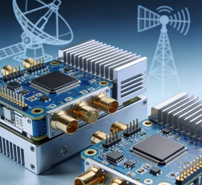
Each self-driving car or smart factory site functions like a small data center. These units create terabytes of raw data for instant analysis. Without fast transceivers, this data piles up. It causes major delays in digital flows. Proper handling keeps operations smooth.
AI training depends on steady processor links. Signal delays slow the entire learning cycle. Hardware must cut wait times to maintain effective feedback. This setup supports efficient model development. It ensures timely responses in applications.
Real-time processing demands instant action. In 6G setups or fast industrial systems, one millisecond separates good results from issues. Networks handle data surges without losing packets or gaining excess heat. They maintain steady performance. This reliability supports critical tasks.
Finding a partner for this setup is key. DEEPETCH emerges as a strong leader in the field. From 2019, they apply the IDM (Integrated Device Manufacturer) approach. This covers chip design to full assembly. Such control speeds up processes over rivals who send out work. For 400G/800G optical modules or TR modules in satellite systems, their full integration ensures top quality and short waits. They have aided over 1,560 clients worldwide. This shows their method succeeds in practical electronics.

Designing and building chips in-house avoids gaps between teams and plants. The end result matches the original plans closely. This direct process boosts accuracy. It leads to dependable products.
Quality comes from planned steps. Adhering to IATF 16949 and ISO 9001 means thorough checks for each part. This delivers lasting performance in tough industrial settings. It builds trust in the components.
Standard parts often fall short for specific needs. The IDM structure enables fast changes from idea to prototype. It skips long delays from external makers. This quick path aids innovation. It fits urgent project timelines.
Fast data creates warmth. Running 800G modules makes heat control a main concern. Substrate and packaging materials must stay steady under load. They prevent failures in use.
New transceivers apply liquid cooling or better heat sinks. Silicon (Si) substrates work well here. They endure high heat up to 1414°C. This base supports complex CMOS tasks reliably. It keeps modules running cool during heavy loads.
Higher frequencies increase signal noise. Materials with strong electron mobility are essential. Gallium Arsenide (GaAs) excels with 8500 cm²/(V*s) mobility, far above silicon. This suits high-speed signals perfectly. It ensures clean data transfer over distances.
Designs shrink while gaining power. Ceramic packaging protects inner circuits in tight spaces. It balances size with output needs. This trend drives efficient builds. It meets demands for compact systems.
In Aerospace and Satellite Communication, demands rise sharply. Parts face radiation and wide temperature shifts. TR (Transmit-Receive) modules form the core support. They enable vital functions in harsh spots.
These chips drive radar operations as key elements. They shift from transmit to receive in mere nanoseconds. GaAs substrates resist radiation well in space vacuum. This choice enhances durability. It supports precise signal handling.
Combining functions cuts weight effectively. A single TR module merges tasks to lower satellite or UAV mass. Each gram saved reduces launch expenses. This integration streamlines designs. It fits budget constraints.
Radar and satellite signals battle interference. TR modules employ detailed filters for clear paths. They work through storms or noisy areas. This processing maintains accuracy. It ensures reliable communication links.
In B2B settings, access to products matters greatly. Supply issues occur often. A partner with massive stock of chips protects your timelines. It prevents project halts.
Delays on sensors should not stop big projects. A broad stock of active and passive parts avoids shortages. This ready supply keeps work flowing. It supports steady production rates.
Moving electronics over borders poses challenges. Networks in places like Shenzhen, Beijing, and Hong Kong speed customs and delivery. Parts arrive promptly at your site. This efficiency cuts wait times. It aids global operations.
Factories must adjust from small runs to large ones. A flexible EMS (Electronic Manufacturing Service) handles this shift well. It moves from prototypes to full output without issues. This scalability meets varying needs. It ensures timely scaling.
Tech advances swiftly. Today’s top tools become common soon. Seek options that address current issues and prepare for 1.6T modules plus 6G. They extend system life. They adapt to changes.
Hardware pairs with software for best results. In 6G and AI, joint design optimizes output. It makes systems both quick and intelligent. This teamwork enhances overall function. It drives better integration.
Energy use draws more attention now. Gallium Arsenide or Silicon-on-Insulator (SOI) lowers module power needs. Savings grow in big data centers. These choices promote green practices. They cut operational costs.
Issues may arise anytime. A partner with direct contact and technical consultation provides help. It turns purchases into ongoing aid. This support builds lasting ties. It resolves problems fast.
Q1: Why is Gallium Arsenide used instead of Silicon in some transceivers?
A: GaAs has much higher electron mobility and is a direct bandgap semiconductor. This makes it faster and more efficient for the light-to-electric conversion needed in high-frequency optical communication.
Q2: What is the benefit of the IDM model for a buyer?
A: It gives you better quality control and faster customization. Since the company designs and manufactures the chips in-house, they can fix issues or change designs much quicker than a company that relies on outside factories.
Q3: Can these transceivers handle the heat of a 24/7 AI computing center?
A: Yes, especially those equipped with liquid cooling solutions. High-quality silicon substrates and advanced ceramic packaging are used specifically to manage the intense thermal output of 800G modules.
Q4: Do you provide parts for satellite and aerospace use?
A: Absolutely. The TR transceiver chips and modules are specifically designed for high-reliability environments like satellite communication and radar, where radiation resistance is a requirement.
Q5: How do I know if the chips I need are currently available?
A: You can check the live stock levels on the website or reach out directly. Keeping a large inventory of chips in stock is a priority to help clients avoid supply chain delays.

The DE-CW-1310 DFB EPI wafer, a high-performance epitaxial structure designed for distributed feedback (DFB) lasers operating at 1310 nm....

Ceramic thin-filmvacuum sensor Optical gas massflowmeter Liquid mass flowmeter Force sensor MEMS...

Photoelectric sensing chip Light source chips Optical transmission and modulationchips Optical detection and receptionchips...

Using a“Detach Core”which has two-layers carrier foil structure on the surface as a core, and forming...

Tenting process is a kind of subtractive process, the process as follows: Laminating photosensitive film...

Modified Semi-Added Process abbreviated as mSAP, which can be used on the core or build-up layers, pattern...

Semi-Added Process abbreviated as SAP, using on the build-up-layer pattern forming as follow:First depositing...

The product generally adopts the pressing lamination process of semi-curing sheets , and line formation...

The products generally adopt the Build-up Film Lamination process, and the circuit formation uses the...

Equipment features: 1. Non-destructive precision testing Micrometer-level probe contact technology...