The shift from 5G to 6G represents more than a simple increase in speed, since it marks a fundamental change toward the Terahertz (THz) spectrum. For worldwide developers, this advance brings notable hardware difficulties that usual production methods cannot address. A collaborator that goes beyond basic assembly is essential, as such a partner combines thorough material knowledge with sophisticated micro-electronics to maintain signal quality at levels where even a tiny micron error causes major degradation.

Projects in this area often face delays because of production barriers. Selecting a top-tier collaborator such as DEEPETCH, founded in 2019, proves vital. This company has expanded 400G/800G high-speed optical modules successfully, and it continues to progress 1.6T research and development. With service to more than 1,560 customers around the world, the IDM model and skills in customized substrates deliver the broad-bandwidth, reduced-delay options that 6G systems require.
Entering the Terahertz range involves wavelengths that are extremely short, so the material traits of PCBs and parts control overall effectiveness. Standard FR4 bases do not work well, because their electrical loss at elevated frequencies causes signal weakening that stops devices from operating properly.
Devices for 6G function in ranges where environmental and material absorption of signals proves strong. Production methods that cut down on electromagnetic disruption and aid accurate THz wave movement become necessary. These processes ensure that hardware meets the demands of such high-frequency operations.
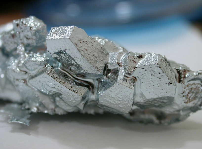
Substances such as Gallium Nitride (GaN) or Indium Phosphide hold importance due to their superior electron movement. Developers also need to evaluate improved glass or ceramic bases, which provide reduced electrical loss and stronger heat resistance than common plastic types. Such choices support reliable performance in demanding conditions.
As 6G units become smaller, combining RF elements calls for accuracy that exceeds typical SMT limits. Reaching line/space details as narrow as 7/8 um often proves required for packaging types like FCBGA. This level of detail maintains functionality in compact designs.
The transceiver forms the central part of every 6G setup, since it needs careful coordination between RF analog output and digital computation strength. Reliance on divided supply networks falls short, so a production process where chip planning and packaging bases develop together works best to reduce unwanted capacitance.
System-in-Package (SiP) enables the combination of various chip functions into one unit, which supports 6G TR modules effectively. This method shortens connection paths, and thereby it keeps signal strength intact at rates of 100GB/S or higher. As a result, overall system efficiency improves significantly.
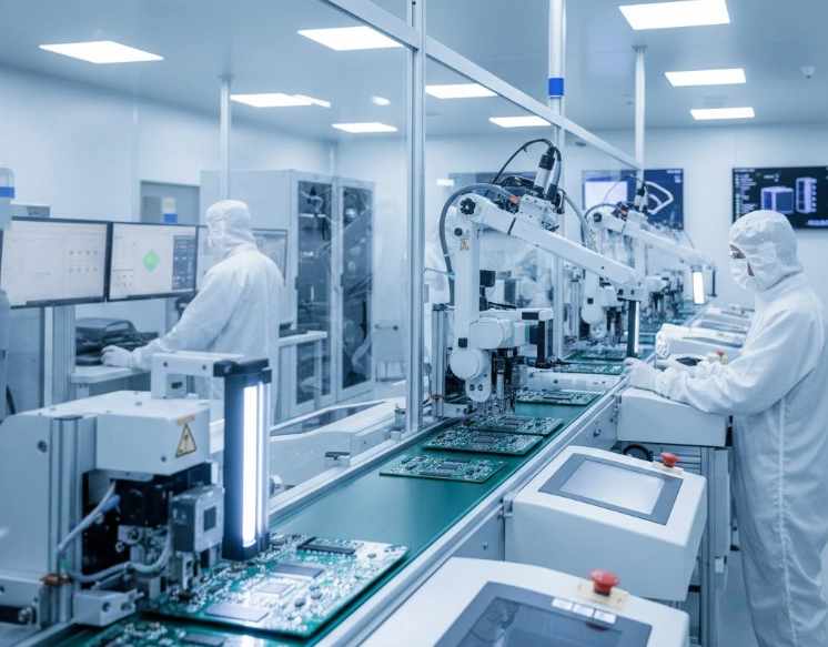
Hardware for 6G requires placement accuracy down to the micron level for components. Systems like advanced AOI, which employ timed position signals, become essential to spot errors at scales below microns and achieve yields of 92% or better. These tools contribute to consistent quality across production runs.
Preparing designs for future use involves readiness for 1.6T data speeds. Equipment specialized for testing must manage Ethernet and InfiniBand standards, while it also keeps power use low. Such testing verifies that modules perform reliably under intense loads.
Elevated frequencies generate dense heat, particularly in small 6G stations or satellite units. Without handling heat control at the base material stage, parts face early breakdown or shifts in frequency from heat-related expansion.
In AI systems and 6G centers, Liquid Cooling High-speed Optical Modules offer effective options. These approaches control the heat from 800G and 1.6T transceivers, which ensures steady operation during peak usage. Consequently, system longevity increases in challenging settings.
Substances like Aluminum Nitride ceramics set new benchmarks with heat conduction up to 170W/MK. They lower resistance to heat flow, and thus they avoid concentrated hot areas that harm delicate 6G detectors. This protection enhances overall device safety.
Hardware for 6G functions in tough spots, from external structures to orbital paths. Endurance against temperatures from -55°C to +175°C without losing form remains crucial. Such robustness guarantees performance in varied environments.
The detailed nature of 6G hardware shows that a basic contract production approach often moves too slowly and lacks flexibility. The greatest gains come from a collaborator following an Integrated Device Manufacturer (IDM) approach, where wafer processing, packaging, and evaluation occur in unified facilities.
Direct links between research teams and production allow early use of DFM (Design for Manufacturing) methods. This connection speeds up changes to 6G samples, and it eases moves to large-scale output. Therefore, development timelines shorten effectively.
6G underpins the Internet of Everything framework. Tailored sensor options, such as MEMS for pressure and gas levels, enable creation of intelligent, 6G-linked devices in industry or healthcare. These integrations expand application possibilities widely.
Worldwide shortages threaten 6G progress. Availability of a robust inventory of high-speed chips and a stable supply network keeps projects on track, even amid market changes. This reliability supports uninterrupted advancement.
In 6G and aerospace fields, errors find no place. A production collaborator must follow the toughest worldwide quality controls to confirm that each TR module or satellite PCBA works as planned during real use.
Collaborators need full approvals, including IATF 16949 for vehicle dependability and ISO 9001 for overall standards. These guidelines ensure that methods for 6G hardware stay uniform and managed. As such, output quality remains high consistently.
Tracking proves key for issue review. Documentation of every part in 6G transceivers, from initial wafer batches to final optical checks, offers complete visibility. This detail aids in swift problem resolution.
Strict checks for shaking, impacts, and resistance to mediums confirm hardware survival in satellite launches or UAV movements. This reliable packaging distinguishes top EMS from basic consumer work. It upholds standards for critical uses.
The 6G period calls for more than a simple producer; it needs a technical supporter able to manage details of Terahertz levels and very fast data flow. Through combining superior materials, exact assembly, and strict heat control, hardware obstacles of the coming phase can be overcome.
Partners providing OEM, ODM, and JDM options let customization of 6G setups at chip and system stages. This adaptability proves vital for leading in the fast-changing telecom sector. It fosters ongoing progress and market edge.
From 10G to 800G and into the 1.6T future, a single provider for optical modules, AOCs, and fast cables eases buying and assures full system match. This setup streamlines operations across projects.
Readiness to address 6G hardware issues involves talks with specialists holding strong records in fast connectivity. Securing a role in communication’s future depends on focusing on quality, fresh ideas, and deep technical skill in EMS ties.
Q1: What are the main material challenges in 6G hardware manufacturing?
A: The primary challenge is signal loss at Terahertz frequencies. You must use low-loss substrates like GaN, SiC, or specialized ceramics to maintain signal integrity.
Q2: What is the benefit of the IDM model for a 6G project?
A: The IDM model provides vertical integration, allowing for faster R&D cycles, better cost control, and seamless coordination between chip design and final assembly.
Q3: Can these high-end EMS services support aerospace-grade reliability?
A: Yes, by adhering to IATF 16949 and ISO 9001 standards and utilizing hermetic sealing and anti-radiation materials, these services meet mission-critical requirements.

The DE-CW-1310 DFB EPI wafer, a high-performance epitaxial structure designed for distributed feedback (DFB) lasers operating at 1310 nm....

Ceramic thin-filmvacuum sensor Optical gas massflowmeter Liquid mass flowmeter Force sensor MEMS...

Photoelectric sensing chip Light source chips Optical transmission and modulationchips Optical detection and receptionchips...

Using a“Detach Core”which has two-layers carrier foil structure on the surface as a core, and forming...

Tenting process is a kind of subtractive process, the process as follows: Laminating photosensitive film...

Modified Semi-Added Process abbreviated as mSAP, which can be used on the core or build-up layers, pattern...

Semi-Added Process abbreviated as SAP, using on the build-up-layer pattern forming as follow:First depositing...

The product generally adopts the pressing lamination process of semi-curing sheets , and line formation...

The products generally adopt the Build-up Film Lamination process, and the circuit formation uses the...

Equipment features: 1. Non-destructive precision testing Micrometer-level probe contact technology...