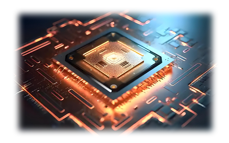
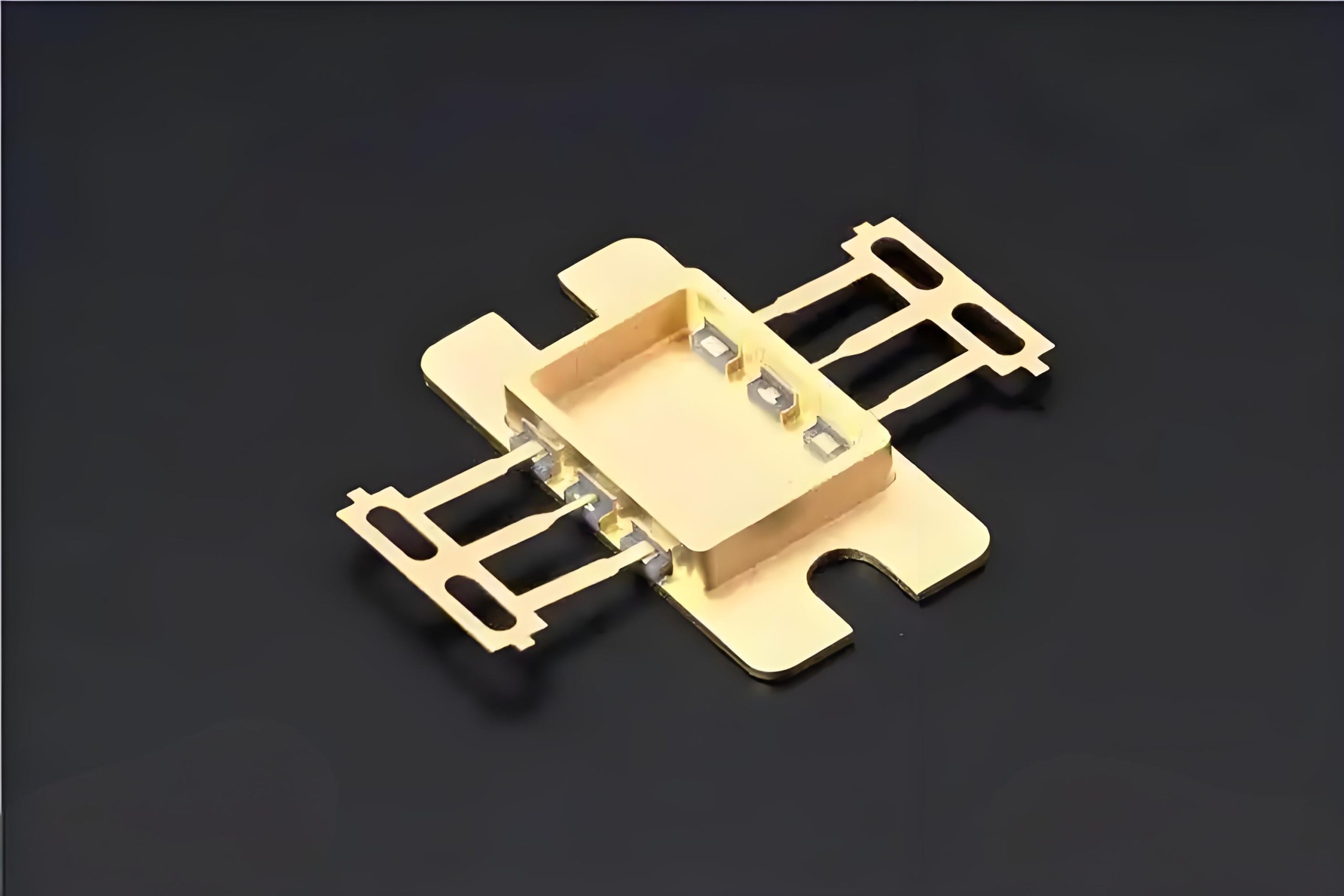
ABF (AJINOMOTO BUILDUP FILM) is a high performance epoxy laminate film, mainly used for high density interconnect (HDI) and advanced packaging, FCBGA (flip chip ball grid array), 2.5D/3D IC packaging.
- Resin system
Modified epoxy resin: with low dielectric constant (DK) and low loss factor (DF), suitable for high frequency signal transmission.
Inorganic fillers (such as SIO₂): adjust the coefficient of thermal expansion (CTE), improve mechanical strength and dimensional stability.
- Reinforced materials
No glass fiber cloth design: Unlike FR-4, ABF uses pure resin film to ensure ultra-thin (1060ΜM) and high flatness.
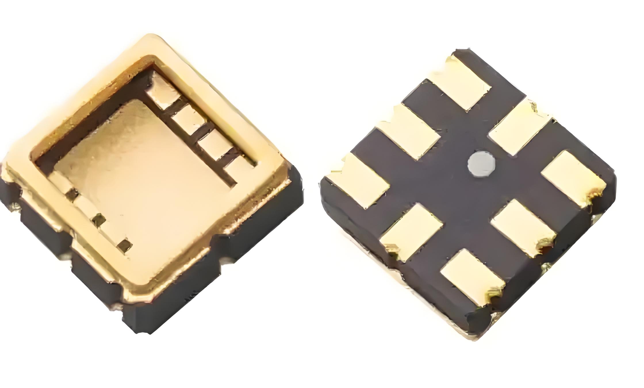
- Copper foil (conductive layer)
Ultra-thin electrolytic copper foil (312ΜM): Chemical oxidation treatment (such as browning) is used to enhance the adhesion to ABF film, so as to achieve high density lines (line width/line distance can reach 5ΜM) for high precision circuit wiring.
Fine lines are made by semi-addition method (SAP) or improved semi-addition method (MSAP).
- Other additives
Photoresist (for laser direct imaging LDI): improves the accuracy of graphics.
Fire retardant (some models): meets the safety requirements of specific applications.
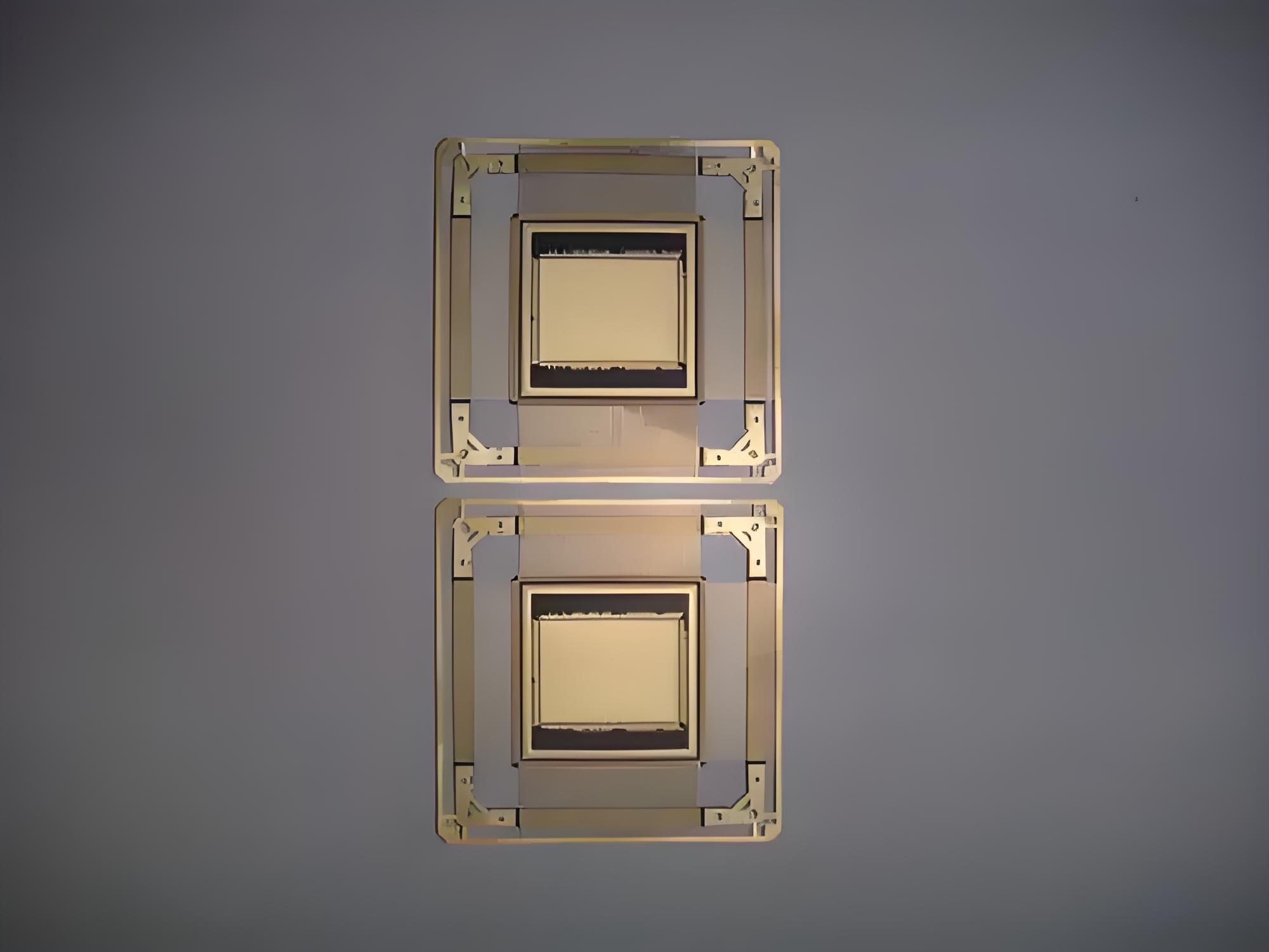
- Substrate pretreatment: The oxide layer on the surface of copper foil is removed by microetching and chemical cleaning to improve the bonding force with ABF film.
- Layered film coating: ABF film is laminated to the substrate surface, and bubble-free bonding is achieved through vacuum hot pressing process (temperature 180200℃, pressure 2030KG/CM²).
- Laser drilling and patterning:
The CO₂ laser drilling (hole diameter 50150ΜM) was used to form a micro-conducting hole.
Dry film lithography (LDI laser direct imaging) can realize high precision circuit pattern transfer, and the line width accuracy can reach ±5ΜM.
Electroplating and etching:
Chemical copper plating (12ΜM) + electroplating thickening (2030ΜM) to fill the hole wall.
Acid etching (FECL₃ or CUCL₂ system) removes excess copper layer and retains the designed circuit.
- Surface treatment: ENIG (chemical nickel gold) or OSP (organic soldering film) process is used to improve welding reliability and oxidation resistance.
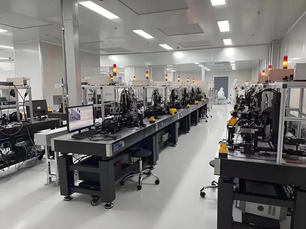
- Testing and Testing:
Performance testing: electrical performance, thermal performance and other aspects of ABF substrate testing
Appearance inspection: The ABF substrate after grinding is inspected for defects, bubbles and other problems
- Material performance advantages
The core performance advantages of ABF substrate are reflected in the following aspects:
Electrical performance:
Low dielectric constant (DK≈3.54.0) and low loss factor (DF≈0.0080.015@10GHZ) are suitable for high frequency signal transmission, reducing signal delay and distortion.
The insulation resistance is greater than or equal to 10¹²Ω·CM, and the breakdown voltage is greater than or equal to 3KV(0.1MM insulation layer), which meets the requirements of high reliability.
hot property:
The glass transition temperature (TG) can reach 200℃, and the coefficient of thermal expansion (CTE) is highly matched with the chip (Z-axis CTE≈50PPM/℃), which reduces the failure caused by thermal stress.
Mechanical and process compatibility:
Ultra-high wiring density (supports <10 ΜM line width, compatible with advanced packaging), supports 1420 layers of high-density interconnects, with line density up to 5 ΜM, suitable for advanced packaging technologies (such as CHIPLET). Compatible with SMT reflow soldering process (temperature tolerance 260℃/40S). Excellent heat resistance (TG> 150°C, suitable for reflow soldering process)
- Industry application and technical index advantages
High Performance Computing (HPC):
Supports the packaging of chips such as CPU, GPU and FPGA. For example, Nvidia A100 GPU uses ABF substrate to achieve heat dissipation capacity> 300W.
To meet the high computing power requirements of AI chips, such as A large number of ABF carriers used in supercomputing clusters required for CHATGPT training.
5G Communication and Data Center:
The 5G base station RF front-end module is used, with dielectric loss as low as 0.008@28GHZ, improving signal integrity.
The server motherboard supports 100GBPS+ high-speed interconnection and more than 16 layers.
automotive electronics:
The vehicle ADAS system chip is packaged with a temperature range of 40℃~150℃, which meets the reliability standards of vehicle specifications.
CE:
High-end smartphone SOC packaging, support ultra-thin design (substrate thickness ≤ 0.3MM).
- Technology upgrading:
CHIPLET Technology drives the growth of layers: in 2025, the number of layers of high-end ABF substrate will exceed 20 layers, with an area of 100MM x 100MM and a line width entering the era of 5ΜM.
Complementary glass substrate: Glass substrate has more advantages in heat dissipation and circuit precision, but ABF still dominates the middle and high-end market in the short term, forming a complementary pattern.
- Material innovation:
Environmentally friendly resin: develop halogen-free, bio-based epoxy resin to meet the requirements of EU REACH regulations.
High frequency material modification: further reduce dielectric loss (target DF<0.005@10GHZ) by doping with nano silica.
- Market expansion:
AI and data center demand surge: The global ABF market is expected to reach $6.529 billion in 2028, with a compound annual growth rate of 5.56%.
The acceleration of domestic substitution: Chinese mainland Enterprises (such as Shennan Circuit and Xing Sen Technology) gradually break through the technical barriers and seize market share.
- Supply chain diversification:
The monopolistic ABF membrane supply situation is difficult to change in the short term, and new entrants try to develop alternative materials to spread the risk.
- Core challenges and response strategies
Process yield: the yield of high number of layers and large area substrate is only 5070%, which requires optimization of laser drilling and pressing process.
Cost pressure: The unit price of ABF substrate is as high as $120/M², which needs to reduce the cost through large-scale production and process innovation.
ABF substrates, with their advantages of ultra-high density wiring, low dielectric loss, and ultra-thin flexibility, have become the preferred material for high-end semiconductor packaging (such as FCBGA, 2.5D/3D ICs). In the future, with the rapid development of AI, 5G/6G, and autonomous driving, ABF substrates will evolve towards lower DK/DF, higher integration, and greater environmental friendliness, continuing to lead advancements in advanced packaging technology.


