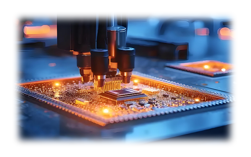
Core advantages of butterfly packaging
- High frequency and high speed signal transmission
Low dielectric loss (TANΔ <0.001): Ceramic substrates (DK≈910) support high frequency signal transmission (up to 40GHZ) and are suitable for RF (RF) and microwave applications.
Short pin design: metal pins are directly connected to the chip to reduce parasitic inductance and capacitance and improve signal integrity (5G millimeter wave module).
- Excellent thermal management capability
High thermal conductivity material: aluminum nitride (ALN) substrate with a thermal conductivity of 150200 W/M·K, can be integrated with copper tungsten (CUW) heat sink, suitable for high power devices (laser diode, GAN amplifier).
Air tight heat dissipation: the fully sealed structure combined with metal heat sink to achieve efficient heat conduction (thermal resistance <5°C/W).
- Environmental reliability and long life
Air tight seal: glass or metal solder seal, leakage rate <1 x 10⁻⁸ ATM·CC³/SEC (helium inspection), moisture-proof and corrosion-resistant, meet MILSTD883 standards.
Wide temperature operation: 55°C to +200°C, suitable for aerospace, military and other extreme environments.
- Photonic integration flexibility
Optical window design: can integrate optical fiber interface or transparent ceramic window, support laser (LD), detector (APD) and other optoelectronic device packaging.
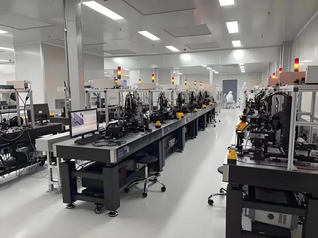
- Prominent technical indicators in industrial applications
| qualification | Typical values/characteristics | Application impact
| frequency range | DC~40GHZ+ | 5G/6G base stations, satellite communications, phased array radar
| Thermal resistance (RTH) | <5°C/W (ALN+ heat sink) | Support stable operation of high power devices above 10W
| Air tightness grade | Helium leak rate <1 x 10⁻⁸ ATM·CC³/SEC | Long life guarantee for aerospace and medical implant devices
| pin configuration | 4~24 pins (coaxial/wire) | Simplify high frequency interconnection and reduce signal reflection loss
| dimensional accuracy | ± 0.05MM (laser alignment) | Sub-micron packaging alignment requirements for optoelectronic devices
Compare other packaging types:
TO coaxial packaging: low upper frequency limit (<18GHZ), comparable heat dissipation capacity but poor scalability.
Plastic QFN: low cost but high frequency loss (TANΔ> 0.02) and insufficient gas tightness.
- The most suitable application scenarios
- Optical communication and laser technology
Lidar (LIDAR): 905NM/1550NM laser package for autonomous driving, which needs to be vibration resistant and high heat dissipation.
High-speed optical module: EML laser for 100G/400G optical communication (gas-tight and anti-oxidation).
- Radio frequency and microwave electronics
5G millimeter wave base station: high frequency, high power packaging (28GHZ/39GHZ) of GAN power amplifier (PA).
Satellite communication T/R module: KA-band phased array antenna module for low Earth orbit (LEO) satellite.
- Aerospace and defense
Electronic warfare (EW) system: X-band radar jamming package.
Missile guidance: microwave integrated circuit (MMIC) package resistant to high temperature and impact.
- Medical and industrial equipment
Medical laser scalpel: stable output package of high power CO₂ laser.
Industrial fiber optic sensing: photoelectric sensors in high temperature environments (oil drilling).
- High frequency and terahertz technology
LTCC/glass ceramic with DK<5: supports 100GHZ+ terahertz communication (6G).
Silicon optical integration: co-packaging of photonic IC and RF devices to reduce power consumption (CPO technology).
- Upgrade of heat dissipation technology
Microchannel liquid cooling: Embedded microfluidic channels to solve the power density challenge of>50W/MM².
Diamond coating: local deposition of diamond, thermal conductivity> 2000 W/M·K.
- Cost optimization and standardization
Scale production: reduce customization costs through standardized pin layout (QSFPDD).
Ceramic 3D printing: rapid prototyping of complex structures and reducing processing steps (hollow heat dissipation design).
- Expansion of emerging areas
Quantum computing: cryogenic gas sealing of superconducting qubits (QUBIT).
Space economy: The need for high reliability packaging is surging for low-cost satellite constellations (STARLINK).
Ceramic butterfly packages, with their high-frequency performance, airtightness, and heat dissipation advantages, hold a core position in advanced fields such as optical communication, defense, and aerospace. In the future, as terahertz communication, heterogeneous integration, and advanced cooling technologies develop, their applications will expand to cutting-edge areas like quantum technology and 6G. Through process innovations to reduce costs, they will gradually penetrate large-scale markets such as automotive electronics (LIDAR).


