Product Introduction
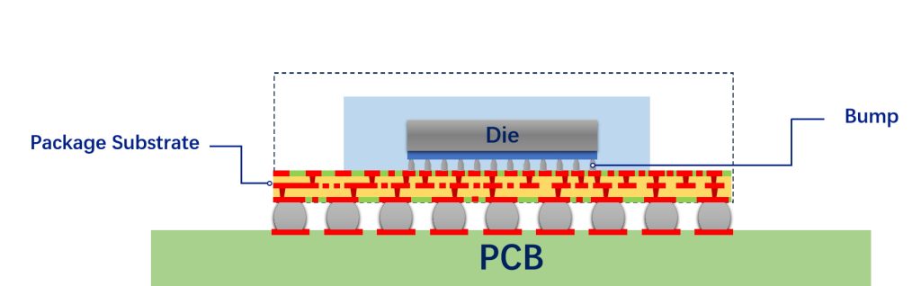
The product generally adopts the pressing lamination process of semi-curing sheets , and line formation uses an improved semi-additive (amSAP) process or subtraction (Tenting) process. The FCCSP (Flip Chip Chip Scale Package) package board in the form of inverted chip packaging for the product.
The features of this type of product include small size, light weight, and relatively fewer layers. They are used in wearable, storage, and RF (radio frequency) applications
Package Structure
Features
|
Smaller micro via by new-generation laser drilling machine AMSAP |
Fine Line/Space by amSAP process |
|
Ultra thin board by Coreless or ETS Process |
Thin Thickness |
Small size |
High Density |
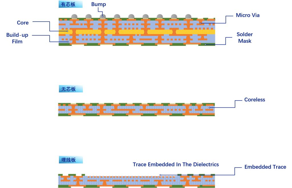
Build-up Structure
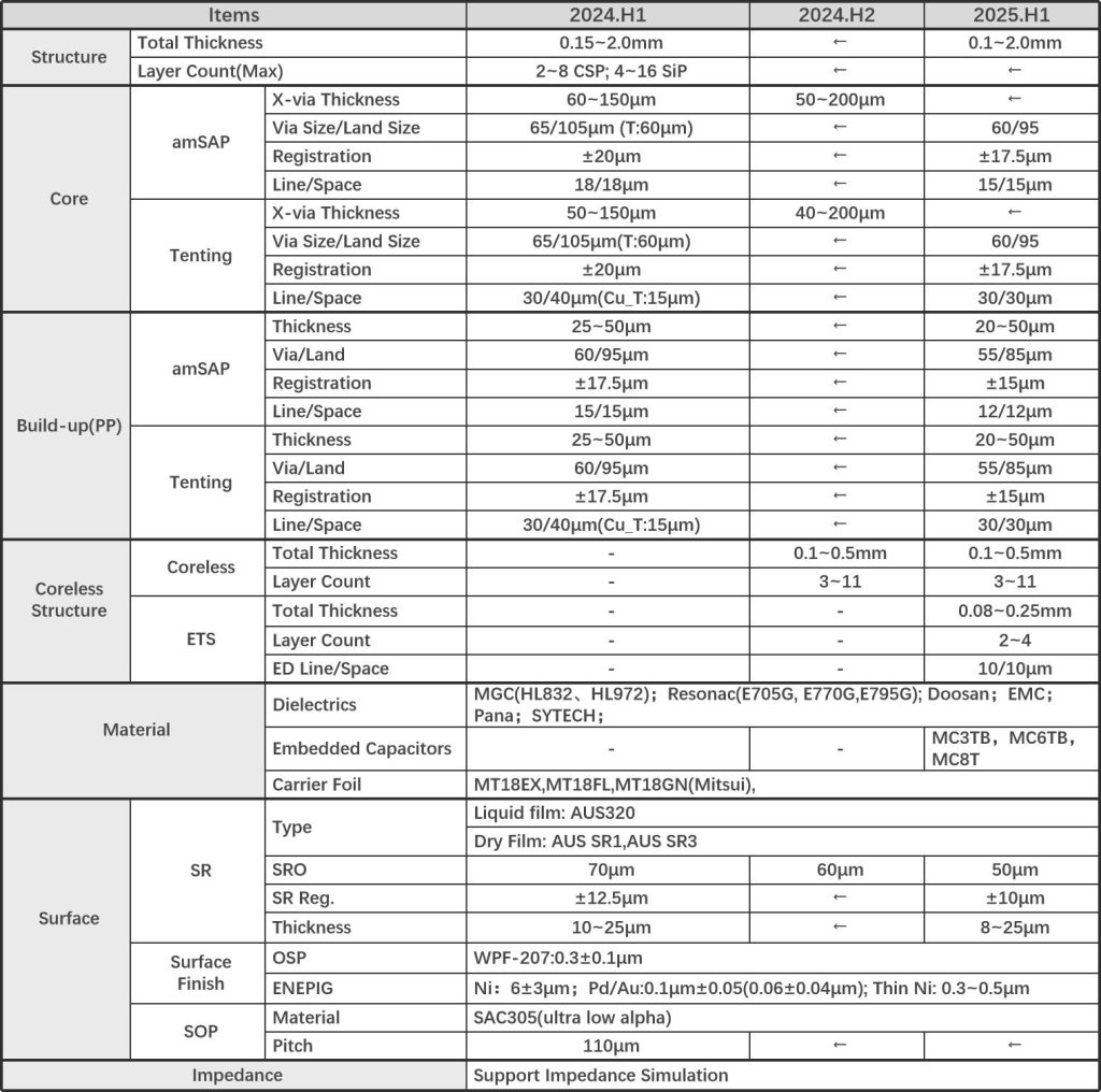
Process Capability
| Process Capability | Applications | |
| · Layer Count: | 2~8 SiP 4~16层 | · AP |
| Board Thickness | · 0.15~2.0mm | · BB |
| amSAP Line/Space | · 15/15μm | · RF |
| Tenting Line/Space | · 40/40μm | · PMIC |
| · Via/Land | Φ55/85μm | · Memory |
| · SRO | · Φ60μm | MEMS & Sensor |
| · SRO/Land Reg | · ±12.5μm | · |
| · Surface Finish | ENEPIG、OSP、ENEPIG+OSP | · |
| Micro bump Pitch | · 110μm | |
| · Coreless | · (2025H1) | |
| · Layer Count | · 3~11 | |
| Board Thickness | · 0.10~1.0mm | |
| · ETS | · (2025H1) | |
| · Layer Count | · 2~4 | |
| Board Thickness | · 0.10~0.25mm | |
| · Line/Space | · 10/10μm | |


The DE-CW-1310 DFB EPI wafer, a high-performance epitaxial structure designed for distributed feedback (DFB) lasers operating at 1310 nm....

Ceramic thin-filmvacuum sensor Optical gas massflowmeter Liquid mass flowmeter Force sensor MEMS...

Photoelectric sensing chip Light source chips Optical transmission and modulationchips Optical detection and receptionchips...

Using a“Detach Core”which has two-layers carrier foil structure on the surface as a core, and forming...

Tenting process is a kind of subtractive process, the process as follows: Laminating photosensitive film...

Modified Semi-Added Process abbreviated as mSAP, which can be used on the core or build-up layers, pattern...

Semi-Added Process abbreviated as SAP, using on the build-up-layer pattern forming as follow:First depositing...

The product generally adopts the pressing lamination process of semi-curing sheets , and line formation...

The products generally adopt the Build-up Film Lamination process, and the circuit formation uses the...

Equipment features: 1. Non-destructive precision testing Micrometer-level probe contact technology...


Title: Semiconductor manufacturing processes Objective: To have a certain foundation for the overall...