FR-4 substrate is a typical representative of glass fiber reinforced epoxy resin composite material, the core structure includes:
Strengthening material: electronic grade alkali free glass fiber cloth (EGLASS) reduces the coefficient of thermal expansion (CTE), with a single layer thickness of 50200ΜM, providing mechanical support.
Resin system: brominated epoxy resin (containing 20% or 30% tetrabromobisphenol A, TBBPA), curing agent (diamino diphenyl sulfone) and toughening agent (rubber particles).
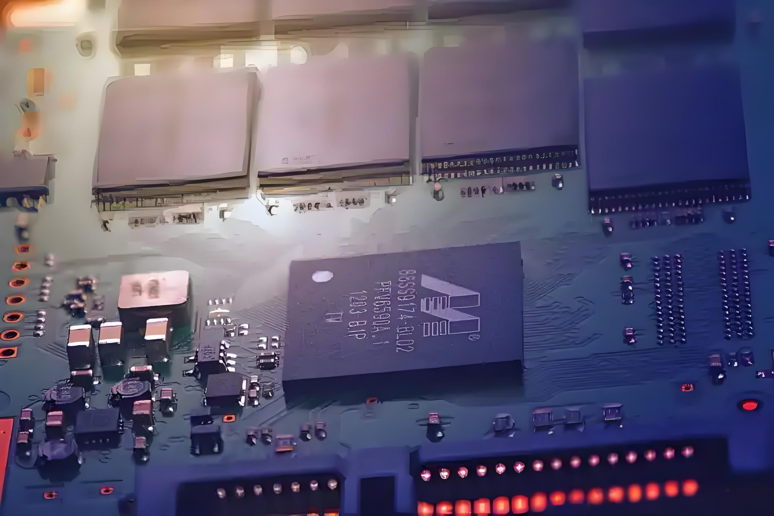
Conductive layer: electrolytic copper foil (ED) or calendered copper foil (RA) (1235ΜM thick), used for circuit wiring, enhanced by chemical oxidation treatment (brown).
Auxiliary materials: flame retardant (to meet UL94 V0 standards), silica micro powder filler (to reduce CTE). Cure agent (DICYANDIAMIDE): to promote resin curing
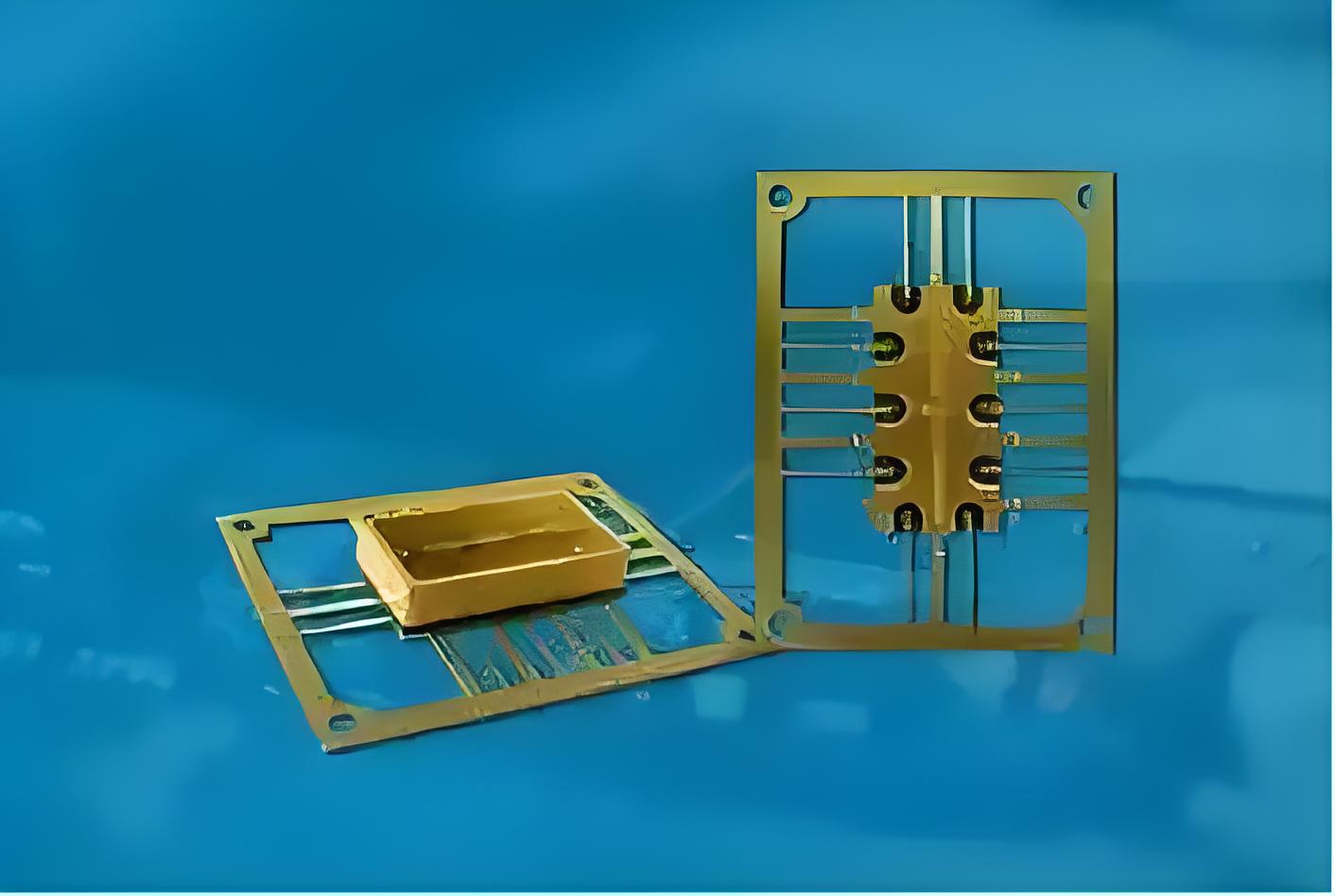
PCB manufacturing (etching, drilling, surface treatment)
1. Preparation of copper clad laminate (CCL)
Prepreg preparation: glass cloth is impregnated with epoxy resin glue (resin content 42%±2%), and cured in vertical oven (80℃→120℃→160℃).
Lamination: multi-layer prepreg is overlapped with copper foil, and vacuum hot pressing is performed (pressure 1525kg/cm², temperature 170185℃, time 90 minutes). Then cut and inspect to form FR-4 copper clad laminate
PCB manufacturing (etching, drilling, surface treatment)
Graph transfer:
Dry film lithography (LDI exposure accuracy ±5ΜM), acid copper chloride etching (CUCL₂+HCL system, side etching control <20%) lithography + etching to form circuit;
machining:
Laminating (multilayer board): Multilayer semi-cured sheet is pressed with inner core board, CNC milling edge (tolerance ±0.1MM).
Drilling: Mechanical/laser drilling to form through-hole (PTH) or micro-hole (HDI)
Electroplated copper: chemical deposition of copper + electroplating of copper to achieve interlayer interconnection.
Outer layer graphics production: the outer layer circuit is completed by secondary lithography and etching.
surface preparation:
Spray tin (HASL), gold deposition (ENIG), OSP, chemical nickel gold deposition (ENIG) or spray tin (HASL, tin layer thickness 13ΜM).
Antioxidation treatment (benzotriazole corrosion inhibitor).
Solder mask (SOLDER MASK) printing: protects non-welded areas
- Material performance advantages
Electrical performance:
Dielectric constant (DK): 4.24.8 (1MHZ1GHZ), meeting the general high frequency requirements.
Loss factor (DF): 0.0150.025 (10GHZ), better than ordinary phenolic substrate.
mechanical behavior:
Bending strength: 400600 MPA (ASTM D790 standard).
Thermal deformation temperature: 130140℃(1.82MPA load).
hot property:
Glass transition temperature (TG): 130180℃ (high TG type can reach 200℃).
Z axis thermal expansion coefficient: 5070 PPM/℃ (25260℃).
Safety performance:
Flame retardant grade: UL94 V0 (self-extinguishing time <10 seconds).
CTI (leakage resistance index): 600V or more.
core advantage:
✅ Low cost (cost-effective mass production)
✅ Excellent electrical insulation (high resistivity, low dielectric loss)
✅ Good mechanical strength (glass fiber reinforced to resist bending)
✅ Mature processing technology (compatible with HDI technology for high density interconnection)
✅ Flame retardant (meeting UL94 V0 standard)
Multi-layer capability: supports 30+ high-density interconnects (line width / line spacing 3/3MIL).
Process compatibility: adapted to SMT reflow soldering (peak temperature 260℃/40S).
Cost efficiency: unit price $515/M², only 1/10 of high-frequency substrate (such as ROGERS 4350).
CE:
Smartphone motherboard (such as IPHONE 14’s 6-layer HDI board), laptop power management module, 4G base station amplifier unit (<3GHZ application).
Fiber optic transceiver circuit board.
industrial computer:
PLC controller I/O interface board, inverter drive circuit.
automotive electronics:
Vehicle information and entertainment system (resistant to 85℃/85%RH environment), body control module (BCM) non-safety related circuits.
Material upgrade:
Halogen-free epoxy resin (CL/BR content <900PPM, in line with IEC 61249221 standard).
Low loss modification (DF decreased to 0.008 @10GHZ, through nano-silica doping).
process innovation:
The MSAP (semi-additive) process achieves a line width of 2ΜM.
Laser direct drilling (LDD) technology is used to process 0.1MM micro holes.
Emerging applications:
Internet of Things terminal equipment (NBIOT module substrate).
Flexible rigid composite plate (FR-4 and PI hybrid structure).
sustainable development:
Biobased epoxy resin (30% castor oil derivative to replace petroleum raw material).
Closed-loop recycling system (glass fiber recycling rate of 85%).
- Market competitiveness analysis
Cost advantage: accounting for more than 60% of the global PCB substrate market share (PRISMARK 2023 data).
Technology substitution: In the 6G millimeter wave era, PTFE substrate challenges are faced, but the dominant position in the medium and low frequency bands is maintained through modification.
Environmentally friendly drive: in compliance with the EU REACH regulations (List of substances under control SVHC, batch 28).
FR-4 substrates, with their mature supply chain and excellent cost-performance ratio, remain a fundamental material in the electronics industry. As 5G REDCAP technology is promoted and Industry 4.0 deepens, the global FR-4 market size is expected to reach $12.8 billion by 2025. Technological advancements will focus on high-frequency, thin-profile, and green manufacturing, continuing to play a core role in automotive electronics non-safety areas and mid-range consumer electronics.


