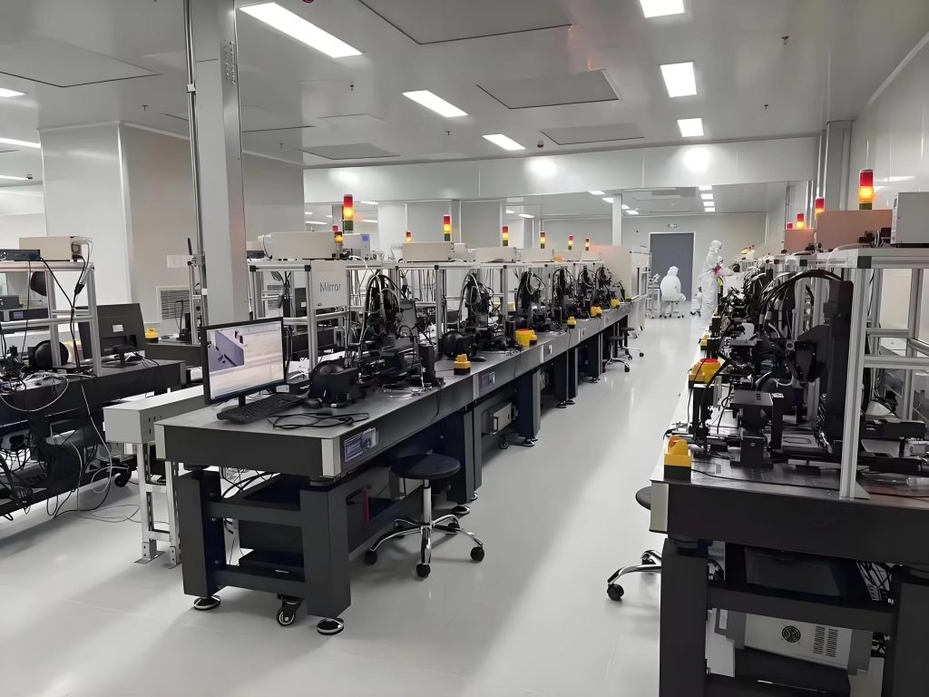
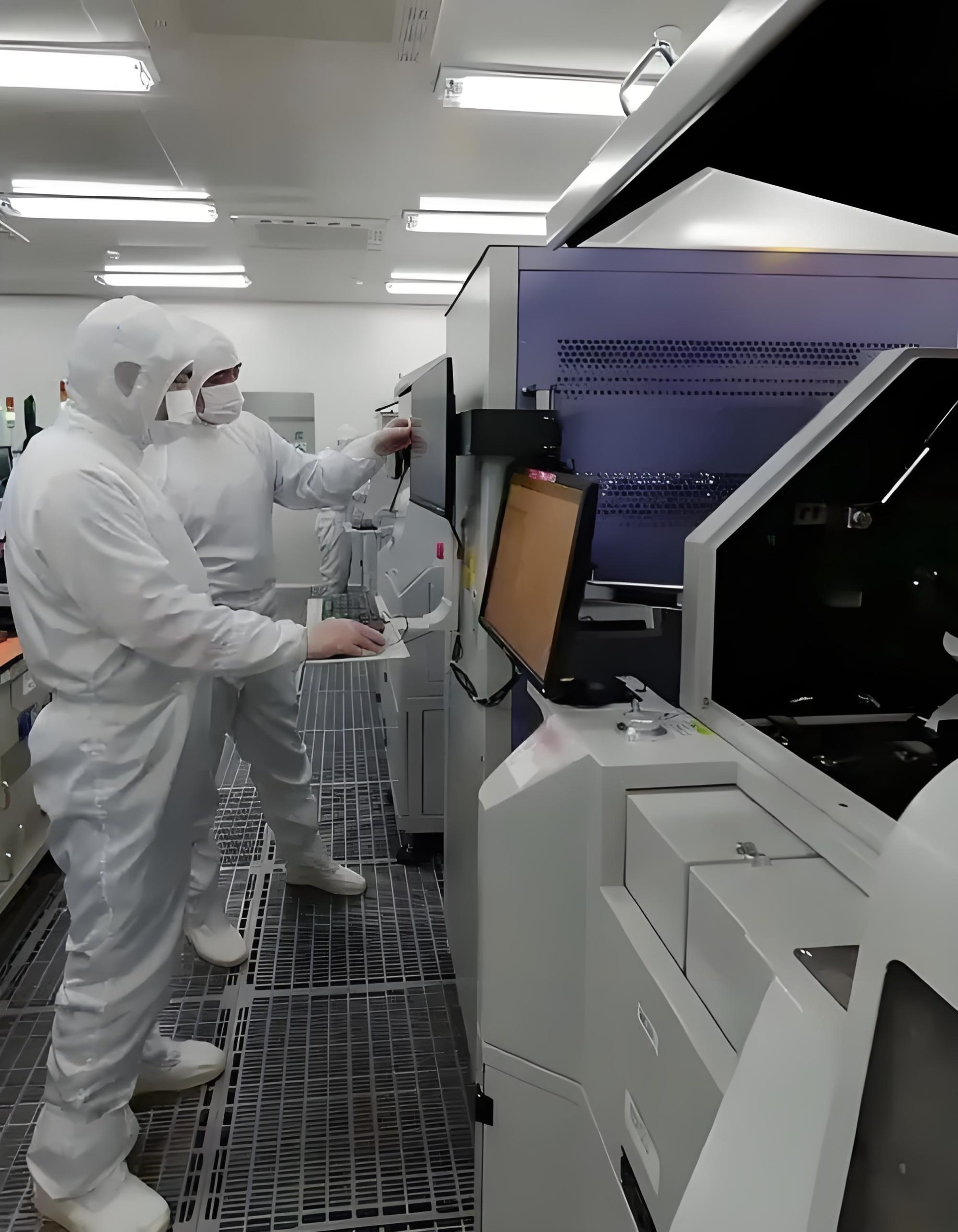
- Manufacturing process of gallium nitride material
- Raw material preparation
High purity gallium (GA) and nitrogen (N) are the main raw materials, and the purity is usually required to be greater than or equal to 99.9999% (6N grade).
- Selection of backing material
Sapphire (AL₂O₃): Low cost, but large lattice mismatch, buffer layer to reduce defects.
Silicon carbide (SIC): good lattice matching, excellent thermal conductivity, suitable for high power devices.
Silicon (SI): Strong compatibility, suitable for mass production, but thermal expansion coefficient differences lead to stress problems.
Self-supported GAN substrate: prepared by HVPE thick film stripping technology, which eliminates the defects of heterogeneous substrate and has the best performance but high cost.
- Crystal growth
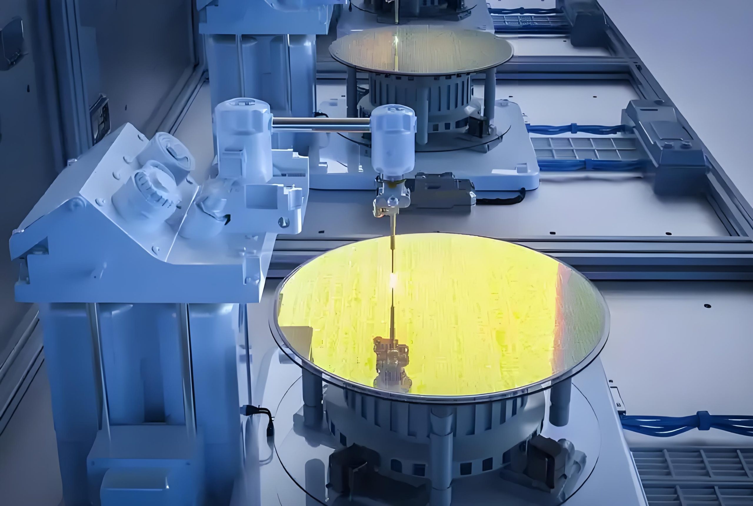
Metal-organic chemical vapor deposition (MOCVD): This process uses metal-organic compounds (such as trimethylgallium) and ammonia (NH₃) to react at high temperatures. Through gas-phase reactions, it epitaxially grows high-quality GAN films on substrates like sapphire, silicon carbide, or silicon. The process takes place at high temperatures (typically 800-1100 degrees Celsius) and high pressures (typically 100-1000 millibars), making it suitable for large-scale production and widely used in the manufacturing of LEDs and power devices
Molecular beam epitaxy (MBE): In ultra-high vacuum environment, gallium and nitrogen atoms are deposited layer by layer through molecular beam to form high quality single crystal thin film.
Hydride vapor phase epitaxy (HVPE): GaCl (GACL) and ammonia (NH₃) are reacted to grow gallium nitride crystals. The growth rate is fast (up to tens to hundreds of microns/hour), suitable for the preparation of thick film substrate materials.
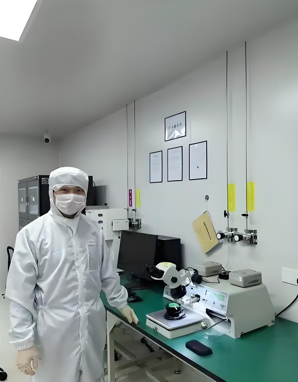
- Wafer processing
The gallium nitride crystal is cut into wafers (typically 150-300ΜM thick) and polished, cleaned and surface treated.
- Doping and device manufacturing
N-type doping: silicon (SI) or germanium (GE) doping, carrier concentration up to 10²⁰ CM⁻³.
Type P doping: Magnesium (MG) doping requires annealing activation to achieve high resistivity (10⁸ Ω·CM).
High electron mobility transistors (HEMT), lasers, LEDs and other devices are manufactured by lithography, etching, deposition and other processes.
Defect control: the dislocation density is reduced by optimizing the growth conditions, substrate pretreatment and epitaxial layer design.
- Packaging and testing
The device is packaged into a chip module and the electrical performance test and reliability verification are carried out.
- Technical index advantages of gallium nitride materials
- High frequency performance
The electron migration rate is up to 2000CM²/V·S, supporting high frequency signal transmission, wide band gap (3.4 EV): high voltage (>600 V), breakdown electric field strength of 3.3 x 10⁶V/CM, much higher than silicon’s 3 x 10⁵V/CM, high saturation electron drift velocity (2.7-5 x 10⁷ CM/S): support high frequency (GHZ level) operation, improve device efficiency, suitable for high power RF devices.
- Power performance
Gallium nitride devices can be switched 10 times faster than silicon-based devices, with 50% lower power consumption, and are suitable for high voltage (above 600V) and large current applications.
- Thermal stability
The thermal conductivity is 130W/M·K, higher than the 150W/M·K of silicon, suitable for high temperature working environment.
- Optical properties
Direct band gap materials (band gap width 3.4EV) are suitable for blue light and ultraviolet light devices, and the light efficiency of gallium nitride based LED can reach 200LM/W, much higher than traditional light sources.
- Low noise characteristics
The noise factor of gallium nitride devices is less than 1DB, which is suitable for low noise amplifiers (LNA).
- Application scenarios of gallium nitride materials
- Power electronics
Power devices: Gallium nitride field-effect transistors (GAN FET) are used in power adapters, electric vehicles and industrial power supplies.
Inverter: Gallium nitride devices are used in solar inverters and motor drives.
- Radio frequency communication
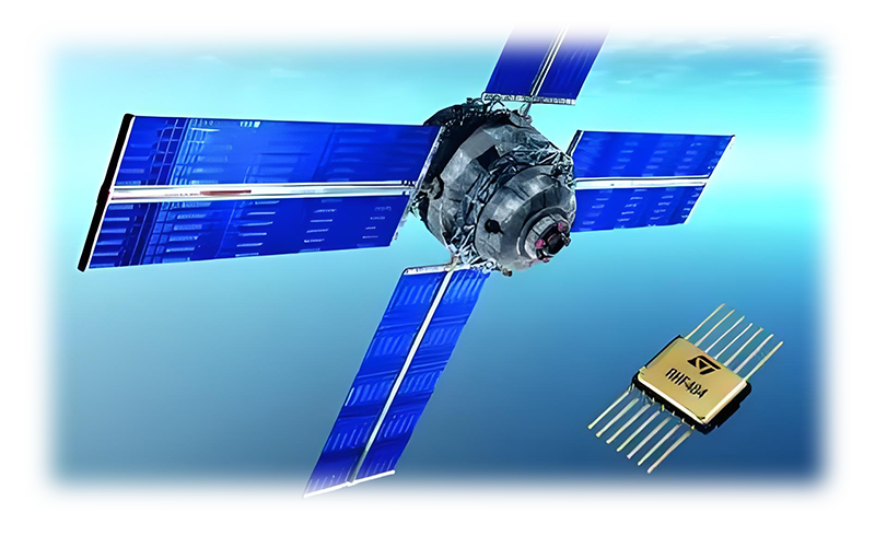
RF devices: Gallium nitride power amplifiers (PA) are used in 5G base stations, satellite communications and radar systems.
Millimeter wave devices: suitable for frequencies above 60GHZ and support high-speed data transmission.
- Optoelectronic devices
LED: Gallium nitride based LED is used for lighting, display and backlighting.
Laser: Gallium nitride lasers are used for blue light storage, laser printing and medical devices.
- Sensors
Ultraviolet detector: Gallium nitride ultraviolet detector is used for environmental monitoring and biomedical testing.
- Competitive advantages of gallium nitride materials
- Power electronics
The power density of gallium nitride devices is five times higher than that of silicon-based devices, which is suitable for miniaturized and high-efficiency power supply design.
- Radio frequency communication field
Gallium nitride PA improves the efficiency of 5G base stations by 30% and reduces power consumption by 40%.
- Optoelectronics
The light efficiency and life of gallium nitride based LED are better than that of traditional light sources, suitable for energy-saving lighting.
- Future development trends
- Heterogeneous integration and cost optimization:
Develop GAN-ON-SI and GAN-ON-SIC technologies to reduce substrate costs and improve heat dissipation performance, and promote large-scale application.
- Intelligent manufacturing technology:
The laser cutting equipment is upgraded to intelligent, and the cutting accuracy is improved to sub-micron level to meet the requirements of complex devices.
- Quantum and new energy applications:
GAN quantum dots are used for single photon sources and quantum computing; photovoltaic electrode technology is expanding to commercial hydrogen production, supporting the carbon neutral goal.
- Development of new devices
Develop flexible gallium nitride devices, terahertz devices and other new devices.
- Application extension
Promote gallium nitride devices in 6G communications, autonomous driving and the Internet of Things (IOT).
Market Expectation: The global GAN power semiconductor market is expected to reach 1.76 billion yuan in 2024 and 50.14 billion yuan by 2028, with a compound annual growth rate of 98.5%. The primary drivers are technological maturity and the surge in downstream demand. Gallium nitride achieves high-quality thin film growth through advanced processes such as MOCVD. Leveraging its wide bandgap and high electron mobility, it holds irreplaceable advantages in high-power, high-frequency, and optoelectronic applications. It will continue to expand, driving innovation in industries such as energy and communications


