The core material of glass substrate is selected according to the application requirements, and the main types include:
- Aluminosilicate glass: high strength and heat resistance, suitable for smart phones, tablet computers and other consumer electronics, strong impact resistance.
- Sodium-calcium glass: low cost and good processability, used for low-end displays and large-size economical equipment.
- Cesium sodium glass: high transparency and low coefficient of thermal expansion (CTE), suitable for high-end display panels (such as OLED, LCD) and precision optical devices.
- Special functional glass: such as flexible glass (for foldable screens) and environmentally friendly lead-free glass (in line with green manufacturing trends).
- Aluminum silicate glass: high mechanical strength, suitable for ultra-thin substrates.
Additives: TIO₂, ZRO₂ and other thermal expansion coefficients may be added, or CEO₂ to enhance the uv shielding performance
- Melt molding: the raw materials are mixed and melted at high temperature (above 1500℃), and then formed by float method (table glass) or pull-down method (ultra-thin glass).
Surface treatment:
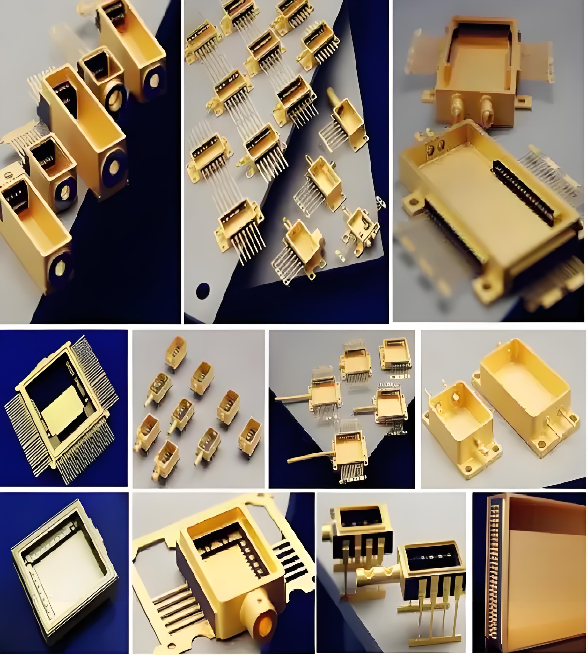
Physical vapor deposition (PVD): For example, Xunlin Technology uses ionized PVD technology to achieve high bonding strength of copper coating (such as copper layer thickness up to 100ΜM) at low temperature, and solve the problem of adhesion between glass and metal.
Chemical strengthening: Surface hardness is enhanced by ion exchange (such as Corning Gorilla Glass).
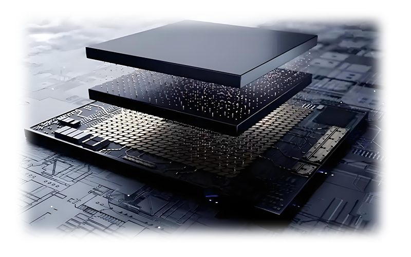
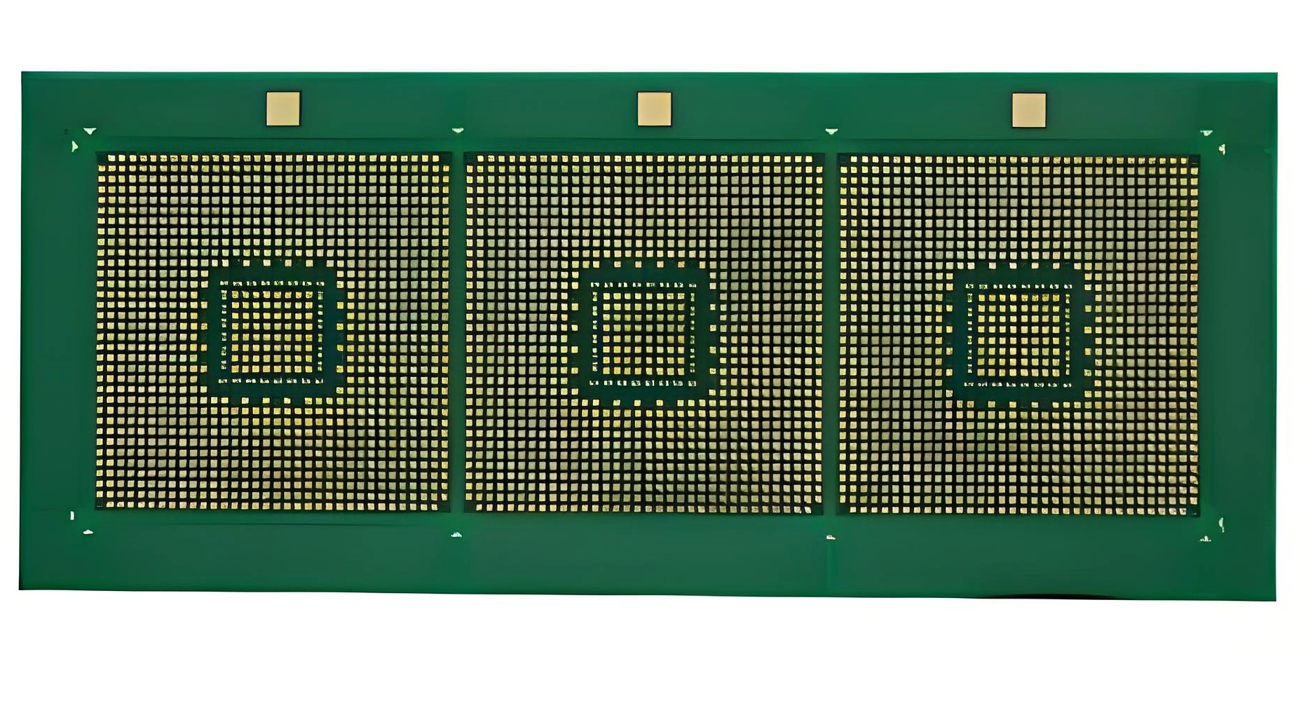
- Glass Through-hole (TGV) process:
Laser induced wet etching: used to form micron-level vias on glass substrates, supporting high density wiring.
Metal filling in the hole: copper paste is used to plug the hole or electroplating process is adopted to ensure conductivity and reliability.
Precision machining: cutting and polishing to a nano-level surface roughness (RA <1NM) for lithography or bonding
- Circuit integration: sputtering metal (CU, AL) or deposition of insulating layer (SIO₂, SINₓ), fine circuit is formed through photolithography and etching to meet the requirements of high density chip packaging.
- Heat treatment: annealing reduces internal stress and enhances mechanical stability.
- Key process challenges: control impurity content, thickness uniformity (within ±1ΜM) and thermal expansion matching.
- Advantages of material properties and technical indicators
The performance advantages of glass substrates make them stand out in many fields:
- Thermal stability and CTE matching: The CTE (3-5 PPM/°C) of glass is close to that of silicon chip (2.6 PPM/°C), and the heat resistance is above 500℃. Large area (500×500 MM² and above) and high flatness can significantly reduce the warping problem in large size packaging, which is suitable for high integration scenarios such as AI computing chips.
- High transparency and low dielectric loss: low dielectric constant (about 5-6), dielectric loss <0.002 (@10 GHZ), volume resistivity>10¹⁴ Ω·CM, suitable for high frequency communication (such as 5G base station RF front end).
- Mechanical strength and weather resistance: elastic modulus of 70-90 GPA, bending strength can reach more than 500 MPA (ultra-thin glass can reach 1 GPA), high temperature (>300°C) and acid and alkali resistance (except HF), no ion migration risk, suitable for automotive electronics and industrial environment.
- Process compatibility: Supports large area (such as 1350 x 1050MM panel) and ultra-thin (<0.1MM) design, suitable for MINI/MICRO LED display technology. Low thermal expansion (<0.5 PPM/°C), high UV transmittance, suitable for photolithography mask
Significant advantages:
- Semiconductor packaging:
AI computing power chip: Glass substrate (such as the glass interlayer planned by Intel) can carry large size chips (> 120MM x 120MM), solve warping problems and improve heat dissipation efficiency.
Power devices: used in electric vehicle inverters and laser headlights, capable of withstanding high power density and thermal shock.
- Display technology:
MICRO LED/MINI LED: Glass substrate supports high precision mass transfer, reduces the thickness of display modules, and improves brightness and contrast.
Transparent screen: used for commercial advertising and on-board display to achieve full transparent visual effect.
- High frequency communication: In 5G/6G base station RF components, the high frequency signal integrity of glass substrate is better than that of traditional PCB.
- Wearable devices: flexible glass substrate is suitable for folding screens and AR/VR devices, taking into account lightness and durability.
- Future development trends
- Technical breakthrough direction:
TGV process optimization: improve the yield of through holes and metal filling efficiency, reduce the cost.
Flexible glass popularization: To promote the development of foldable devices and flexible electronics, it is necessary to solve the problem of bending fatigue.
- Material innovation:
Environmental protection: lead-free, mercury-free materials are used to improve the recycling rate.
Intelligent: integrated self-cleaning coating, light adjustment function, enhance user experience.
- Localization of industrial chain: Chinese manufacturers (such as Xunlin Technology) accelerate the layout to promote the localization of glass substrate production equipment and process.
- Market expansion: After 2025, the penetration rate of glass substrate in IC carrier market will increase significantly, replacing the core layer of traditional ABF carrier.
Glass substrates are rapidly rising in the fields of semiconductor packaging, display technology, and high-frequency communication due to their excellent CTE matching, high-frequency performance, and process flexibility. In the future, with the maturation of TGV processes and breakthroughs in flexible materials, glass substrates will drive electronic devices toward higher integration and thinner designs, becoming the core material for next-generation advanced packaging and display technologies.


