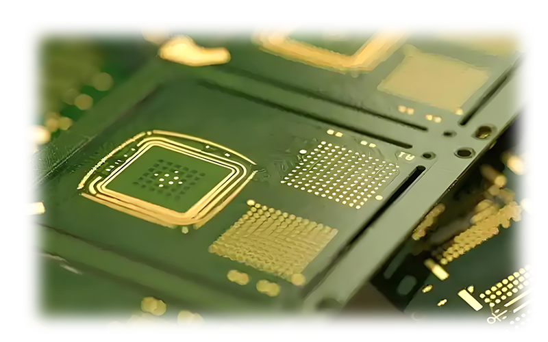
InAS is a III-V compound semiconductor with narrow band gap (0.35 EV) and high electron mobility (33,000 CM²/V·S). Its manufacturing requires precise control of stoichiometric ratio and crystal defects
- The manufacturing process of indium arsenide (INAS)
- Preparation of raw materials
High purity indium (IN) and arsenic (AS) are purified to 99.9999% (6N) or more by vacuum distillation or regional smelting.
Synthesis of INAS polycrystal: IN and AS are sealed in a quartz tube at a molar ratio of 1:1. At high temperature (800-900℃), they are sublimated into arsenic vapor. The arsenic vapor reacts with indium melt in the crystal growth crucible at high temperature to form indium arsenide melt, and then INAS ingot is generated by cooling.
- Thin film preparation
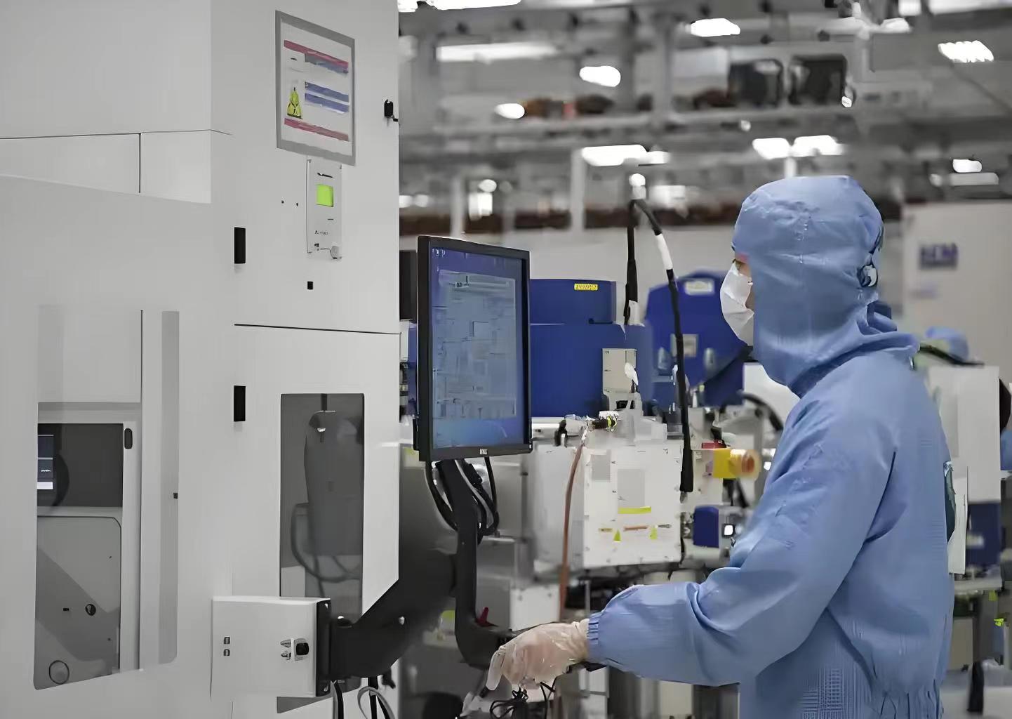
Molecular beam epitaxy (MBE): In ultra-high vacuum (10⁻¹⁰ TORR), IN and AS atoms are evaporated by electron beam to grow high quality single crystal thin films on GAAS, INP or SI substrates, suitable for quantum well and quantum dot structures.
Metal organic chemical vapor deposition (MOCVD): using trimethylindium (TMIN) and arsine (ASH₃) as precursors, INAS layer is deposited at 500-700℃, suitable for large area uniform film preparation.
Bridgeman Method (BRIDGMAN): Used to grow large INAS single crystal ingots, the integrity of the crystal is controlled by a vertical temperature gradient to obtain substrate material up to 3 inches in diameter.
- Post-treatment process
Doping regulation: silicon (SI) as N-type dopant (concentration 10¹⁶-10¹⁹ CM⁻³), zinc (ZN) or carbon (C) as P-type dopant.
Heterojunction preparation: quantum well (such as INAS/GASB superlattice) is formed by combining with materials such as GASB and INGAAS for infrared detector.
Surface treatment: chemical corrosion (such as H₂SO₄:H₂O₂:H₂O mixture) to remove the surface oxide layer to ensure stable device performance.
- Subsequent processing: The grown indium arsenide single crystal is cut, ground and polished to obtain the desired size and surface quality.
- Industry application technical index advantages
- Infrared detector and imaging
Mid-wave infrared response: covers the 3-5 ΜM band, suitable for night vision devices, thermal imaging devices and remote sensing.
High quantum efficiency: more than 80% at room temperature, more stable than cadmium telluride mercury (HGCDTE).
Fast response time: about 10 NS, suitable for high-speed dynamic target detection.
- High frequency electronic devices
High electron mobility: 33,000 CM²/V·S at 300K (8,500 CM²/V·S for GAAS), supports high frequency electronic devices, suitable for millimeter wave (30-300 GHZ) communication devices. Low defect density improves device performance
Low noise characteristics: the noise factor is less than 0.5 DB in HEMT (high electron mobility transistor), which is used for radar and satellite communication.
- Quantum dots and quantum computing
Advantages of zero-dimensional structure: INAS quantum dots have adjustable band gap (0.3-1.5 EV) for single photon emitters and qubits.
Spin-orbit coupling: Strong spin-orbit interaction is conducive to the construction of spin qubits and reduces decoherence effects.
- Thermoelectric conversion
Low thermal conductivity: 0.025 W/CM·K (300K), combined with high electrical conductivity, ZT value (thermoelectric value) can reach 1.5, suitable for thermoelectric power generation.
High temperature stability: the structure is stable below 400℃, which is better than traditional BI₂TE₃-based materials.
- Photovoltaic and optoelectronic devices
Stacked solar cells: as intermediate sub-cells (band gap 0.35 EV), they are composed of three junction cells with GAAS (1.42 EV) and GE (0.67 EV), with an efficiency of over 40%.
Laser diode: INAS quantum dot laser operates at wavelengths of 1.3-1.55 ΜM for optical fiber communication.
- Comparative advantages with other materials
| metric | INAS | GAAS | INSB
| band gap (EV) | 0.35 (direct) 1.42 (direct) | 0.17 (direct)
| Electron mobility (CM²/V · S) | 33,000 (300K) | 8,500(300K) | 77,000(300K)
| Thermal conductivity (W/CM·K) | 0.025 (300K) | 0.46 | 0.23
| Response wavelength (ΜM) | 3-5 (mid-wave infrared) | 0.8-1.8 (near infrared) | 3-5.5 (mid-wave infrared)
| ZT value (thermoelectric) | 1.5 (400K) | 0.4 | 0.7
- Material toxicity: The high toxicity of AS requires strict control of the production environment, and the future may explore the alternative material without AS (INSE).
- Stability problem: INAS is easy to oxidize, so it is necessary to develop antioxidant packaging technology.
- Emerging directions: Terahertz devices: signal processing in the 0.1-10 THz band by using high electron mobility; development of new transistors combined with graphene and molybdenum disulfide.
As a representative of narrow band gap semiconductors, INAS has unique advantages in the fields of infrared detection, high frequency electronics and quantum technology. The application needs in military, communication and energy fields are driving technological innovation. With the development of heterojunction integration and nanotechnology, INAS is expected to become the core material of next-generation semiconductor devices.


