Indium tin oxide (INDIUM TIN OXIDE, ITO) is an important transparent conductive oxide (TCO) material. Due to its excellent conductivity and light transmittance, it is widely used in display technology, solar cells, touch screens and other fields.
- Manufacturing process of indium tin oxide material
- Raw material preparation
High purity indium oxide (IN₂O₃) and tin oxide (SNO₂) are the main raw materials, and the purity is usually required to be greater than or equal to 99.99%.
Mix in proportion (usually 90% IN₂O₃ and 10% SNO₂).
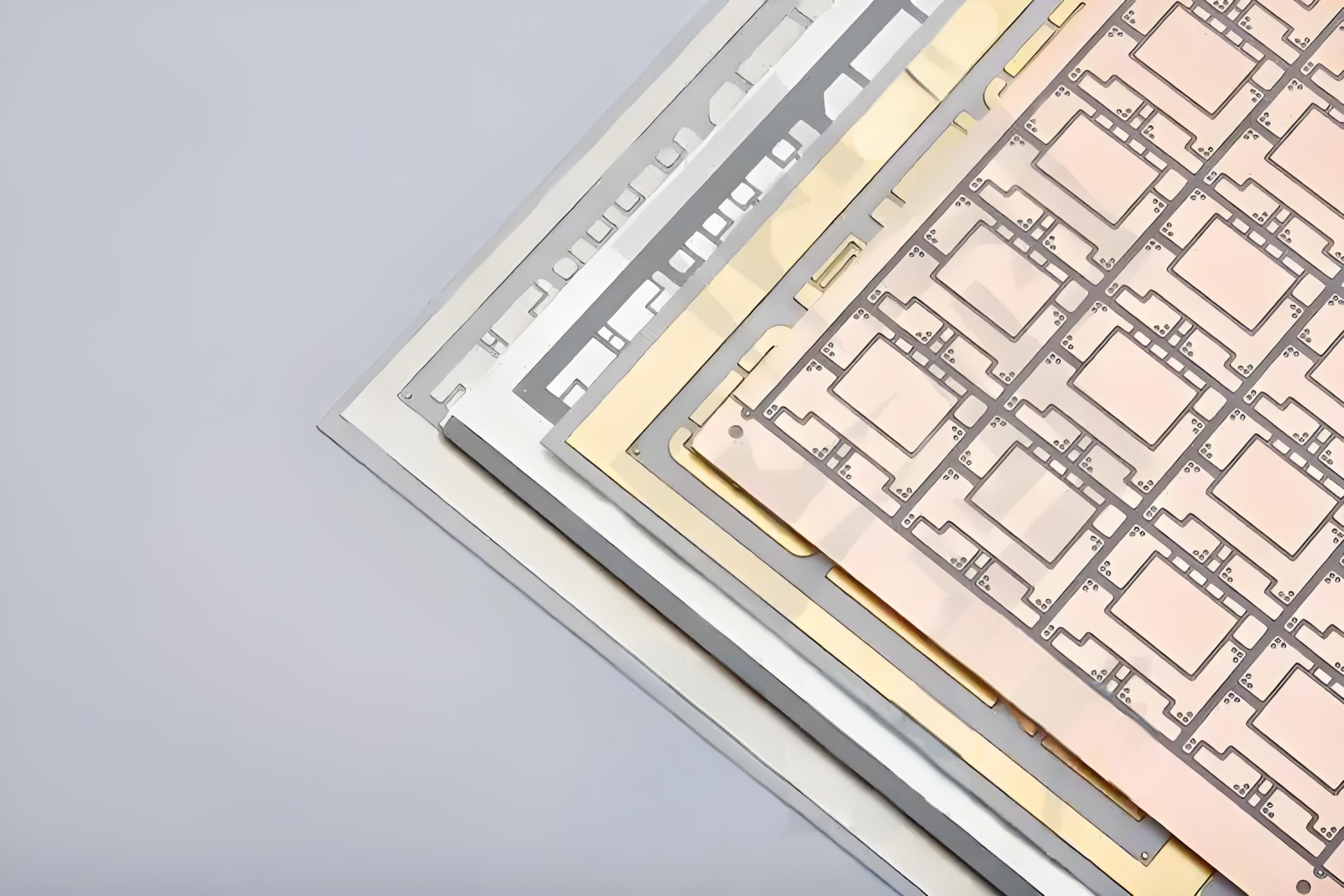
- Film preparation
Magnetron sputtering:
Use IN₂O₃: SN target (usually containing 90% IN₂O₃ + 10% SNO₂) sputtering deposited in argon-oxygen mixed atmosphere.
Process parameters: pressure 0.11 PA, power 100500 W, substrate temperature 100300℃.
Electron beam evaporation:
The IN₂O₃ and SNO₂ hybrid materials were heated and evaporated, and deposited on the substrate in a vacuum environment.
It is suitable for small area and high precision film preparation.
Chemical vapor deposition (CVD):
The precursor (such as trimethylindium and tetrachlorosilicon) reacts with oxygen to form ITO film at high temperature (300500℃).
Suitable for uniform deposition over a large area.
- Annealing treatment
Annealing was carried out at high temperature (300500°C) to improve the crystallinity and conductivity of the film.
- Doping and modification
The electrical performance of ITO was optimized by adjusting the SN doping ratio (usually 510%).
Optical and mechanical properties are optimized by surface modification or nanostructure design.
- Device manufacturing
Transparent electrodes (such as touch screens and solar cells) are manufactured using lithography, etching and other processes.
- Technical index advantages and application
- Transparent Conductive Film (TCO)
The visible light transmittance is>85% (wavelength 400-800 NM). By optimizing the film thickness and refractive index, the reflectivity can be less than 1%, and the resistivity is as low as 15 × 10⁻⁴ Ω·CM. It is the best transparent oxide with the best conductivity at present. The high carrier concentration: electron concentration can reach 10²¹ CM⁻³, and the mobility is 2060 CM²/ (V·S).
Compared with other materials (such as aluminum doped zinc oxide), ITO has a better balance of conductivity and transparency, and is resistant to hydrogen plasma corrosion.
Display technology: Transparent electrodes for LCD and OLED, supporting high resolution and flexible screens.
Solar cells: As electrode materials to improve the efficiency of photoelectric conversion, especially in perovskite cells.
- Infrared and photoelectric characteristics
Low infrared emissivity: The average emissivity of ITO powder prepared by chemical co-precipitation method is only 0.60-0.75 in the 8-14 ΜM band, which is suitable for military infrared camouflage and photoelectric stealth.
Ultraviolet shielding: ITO films can block ultraviolet light, prolonging the life of devices and used in building glass and car coatings.
- Sensors and biomedical applications
Gas sensor: the rich oxygen vacancy on the surface makes the detection limit of NO₂, H₂ and other gases as low as PPB.
Biosensor: The ITO electrode printed by screen printing combined with nano-modified materials can rapidly detect abnormal prothrombin with short response time and high sensitivity.
- Extreme environmental stability
Excellent thermal stability (tolerance to 1400°C high temperature) and suitable for aerospace devices (such as jet engine sensors).
Strong radiation resistance, suitable for high energy physics and nuclear industry environment.
- Compare the core advantages of other transparent conductive materials
| characteristic | ITO | Aluminum doped zinc oxide (AZO) | Carbon nanotubes (CNT)
Visible light transmittance | >85% | >80% | >90%
| Resistivity (Ω·CM) | 10⁻⁴ | 10⁻³ | 10⁻²–10⁻³
| Mechanical flexibility | low | secondary | tall
| prime cost | High (dependent on indium resources) | Low | secondary
| grade of maturity | Industrialization is mature | developing | Laboratory phase
- Challenges and future directions
- Resource constraints: Indium is limited in the earth’s crust (about 0.1 PPM) and expensive, requiring the development of alternative materials (AZO or graphene) or recycling technologies.
- Flexible adaptation: Traditional ITO is brittle and the application of rigid substrate is limited, so it is necessary to combine nanostructure design (silver nanowire composite) to improve the performance of flexible devices.
- High temperature stability: it is easy to decompose above 400℃, which limits its application in high temperature environment
- Process optimization: Develop low temperature and low pressure deposition processes to reduce production costs, such as plasma enhanced chemical vapor deposition (PECVD).
The excellent conductivity, light transmittance, and process compatibility of ITO still set the industry standard for transparent conductive materials, making it irreplaceable in high-end displays and photovoltaic fields. However, the scarcity of indium resources has driven the industry to explore low-cost and environmentally friendly alternatives (such as AZO and graphene). In the future, ITO may complement new materials in specific high-reliability scenarios.


