Introduction
Semi-Added Process abbreviated as SAP, using on the build-up-layer pattern forming as follow:First depositing with a very thin copper seed on build-up film and in micro vias as a conductive layer; Laminating photosensitive dry film resist on the surface; forming the circuits pattern on the dry film using graphic transfer technology(exposure and development); and then metalizing with copper by filling the spaces of dry film pattern; Removing copper seeds between metalizing copper patterns by flash-etching and forming the copper circuits finally.
Compared with other conventional process, SAP Process needs higher level technology control. The process is as follows
Process schematic diagram
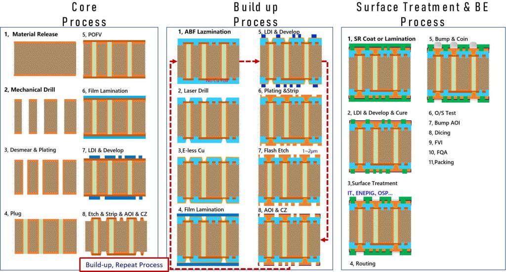
SAP、MSAP and Tenting are three kinds of mainly processes in PCB industry, and each has its own advantages and disadvantages. And the processes are constantly evolving and advancing. In a lot of different applications, the boundaries between the processes are blurred, and could be used in combination sometimes.QHIC has SAP、MSAP and Tenting process with well-rounded technology, and can provide high-quality low-cost solutions according to customers’ needs.


The DE-CW-1310 DFB EPI wafer, a high-performance epitaxial structure designed for distributed feedback (DFB) lasers operating at 1310 nm....

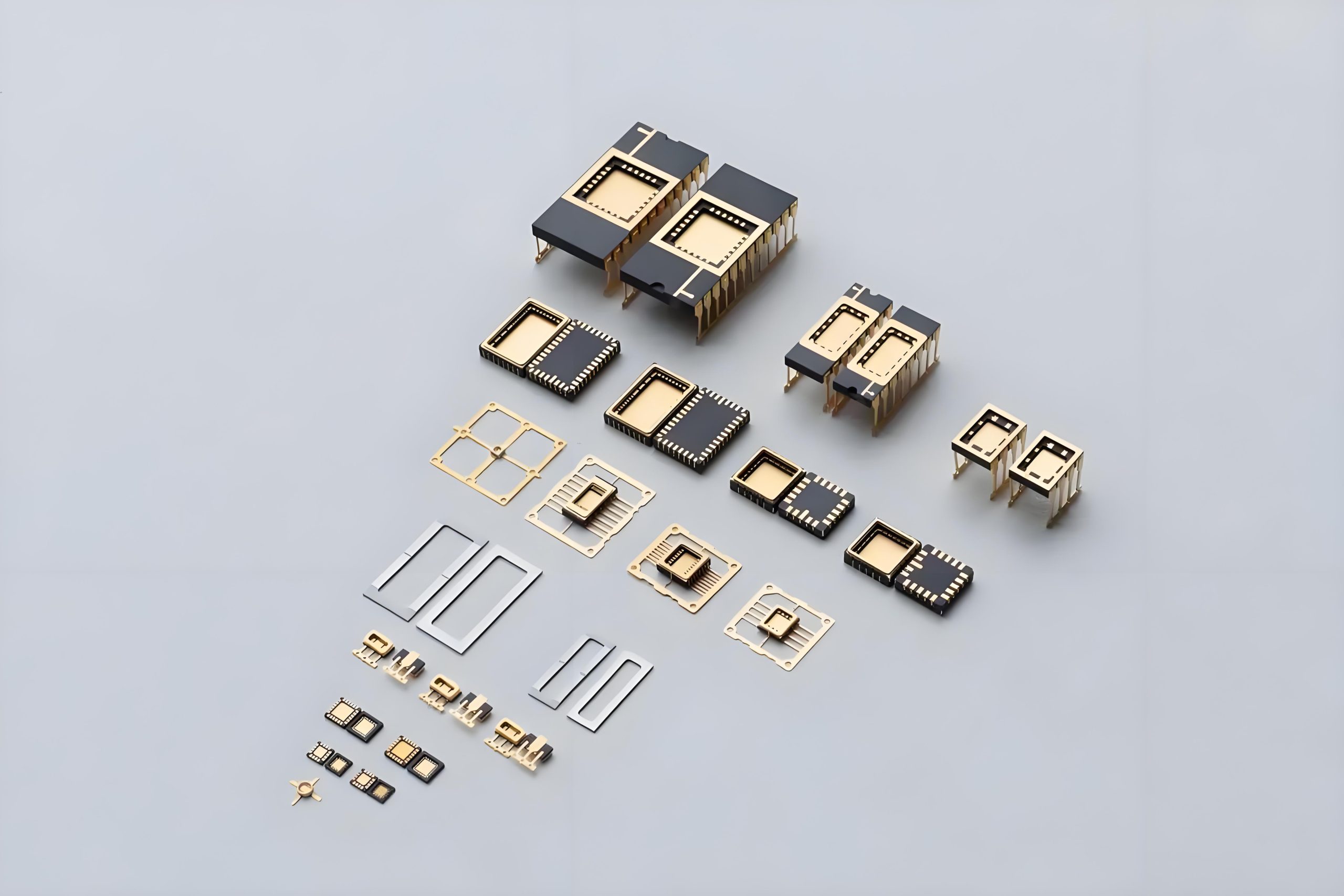
Ceramic thin-filmvacuum sensor Optical gas massflowmeter Liquid mass flowmeter Force sensor MEMS...

Photoelectric sensing chip Light source chips Optical transmission and modulationchips Optical detection and receptionchips...

Using a“Detach Core”which has two-layers carrier foil structure on the surface as a core, and forming...

Tenting process is a kind of subtractive process, the process as follows: Laminating photosensitive film...

Modified Semi-Added Process abbreviated as mSAP, which can be used on the core or build-up layers, pattern...

Semi-Added Process abbreviated as SAP, using on the build-up-layer pattern forming as follow:First depositing...

The product generally adopts the pressing lamination process of semi-curing sheets , and line formation...

The products generally adopt the Build-up Film Lamination process, and the circuit formation uses the...

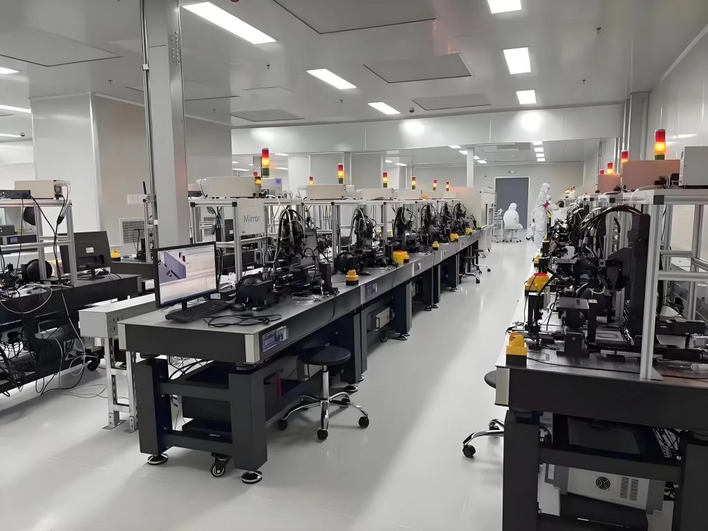
Equipment features: 1. Non-destructive precision testing Micrometer-level probe contact technology...


Title: Semiconductor manufacturing processes Objective: To have a certain foundation for the overall...