SN-CW-1310 DFB EPI Wafer

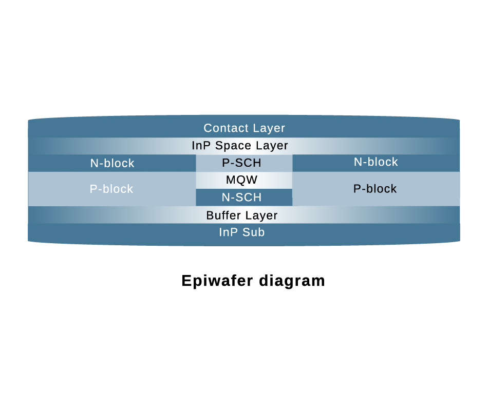
The SN-CW-1310 DFB EPI wafer, a high-performance epitaxial structure designed for distributed feedback (DFB) lasers operating at 1310 nm

  • High uniformity 2/3/4 inch EPI wafer
  • Excellent spectral stability and low phase noise
  • Stable 70mW continuous wave (CW) output power
  • Low threshold current and low drive voltage
  • Excellent temperature stability for wide operating temperature range
  • Optimized for mass production with consistent quality

Typical Epitaxy Parameters

PARAMETER VALUES
PL Wavelength control <5nm
PL Wavelength uniformity Std. Dev < 1nm @inner 42mm
Thickness control < ±3%
Thickness uniformity < ±3% @inner 42mm
Doping control < ±10%
P-InP doping (cm-3) Zn doped ; 5e17 – 2e18
N-InP doping (cm-3) Si doped ; 5e17 – 3e18
AllnGaAs doping (cm-3) 1e17 – 2e18
lnGaAsP doping (cm-3) 5e17 – 1e19
lnGaAs doping (cm-3) 5e14 – 4e19


Typical LD Chip Parameters

PARAMETER SYMBOL TYP UNIT
Peak Wavelength λp 1310 ± 3 nm
Threshold Current Ith < 15 mA
Front Power Po > 9 mW
Slope Efficiency η > 0.45 W / A
Series Resistance Rs < 5 Ohm
Band Width SMSR > 35 dB

Application Areas

  • high-speed optical communication
  • LiDAR

IDM Customization Service

From advanced processes to specialty processes, we use our IDM vertical integration experience to help customers overcome design-process collaboration challenges.

01

Supports advanced nodes such as [5-22nm FinFET/BCD/GAA] to meet the needs of high-performance computing (HPC), AI chips, etc.

02

MPW (Multi-Project Wafer) Service: Small batch trial production to reduce customers' initial costs. Customized process development: Cooperate with customers to conduct DTCO (Design-Process Co-Optimization), customize design rules and process parameters.

03

We support the joint solution of "wafer foundry + advanced packaging" (such as 3D IC, heterogeneous integration) to avoid the loss of multi-supplier collaboration. Unlike pure foundries, we verify the process stability through mass production of our own chips to reduce the risk of tape-out for you.

Provide customers with complete integrated manufacturing services from concept to finished product

01

Electronic manufacturing services and printed circuit board assembly.

02

EMS provides a wide range of electronic manufacturing services, including everything from circuit board design to supply chain management to assembly, testing and after-sales support.

03

PCBA is a link in EMS that focuses on the assembly of printed circuit boards, covering component placement, soldering and related testing, connecting electronic components to manufactured printed circuit boards.

News Center