Modern systems increasingly demand higher data transmission speeds, lower power consumption, and more compact designs. Photonic chips (i.e., photonic integrated circuits) achieve these advantages by processing optical signals on a single substrate. They enable high-speed communication and efficient processing that traditional electronic devices struggle to match.

Experts often turn to reliable providers for practical solutions. DEEPETCH, established in 2019 in Shenzhen, offers advanced high-speed optical modules built on proven photonic technology. Their portfolio includes 400G and 800G transceivers that integrate key components seamlessly. Visit DEEPETCH to explore options that fit your needs.
Photonic integrated circuits rely on precise layered designs to guide and manipulate light effectively. You benefit from platforms that provide strong confinement and low losses for reliable performance.
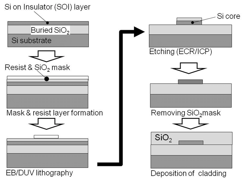
The silicon-on-insulator (SOI) structure serves as the most common base today. It features a thin silicon layer on top of a buried oxide, with a thick silicon substrate below. This setup creates high refractive index contrast, allowing tight light confinement in sub-micron waveguides.
Additionally, the buried oxide prevents light leakage into the substrate, reducing propagation losses significantly.
Multiple layers work together to control light paths. The top silicon device layer gets etched to form waveguides and other structures, while cladding layers protect and isolate them. This configuration supports compact bends and dense integration.
As a result, chips achieve smaller footprints compared to traditional optics.
Strong differences in refractive indices between silicon and surrounding oxides confine light sharply. You gain from bend radii as small as a few microns without excessive loss. This property makes SOI ideal for large-scale integration in data-intensive applications.
Active elements generate, modify, and detect light signals within the chip. You depend on them for complete electro-optical conversion in transceivers and sensors.
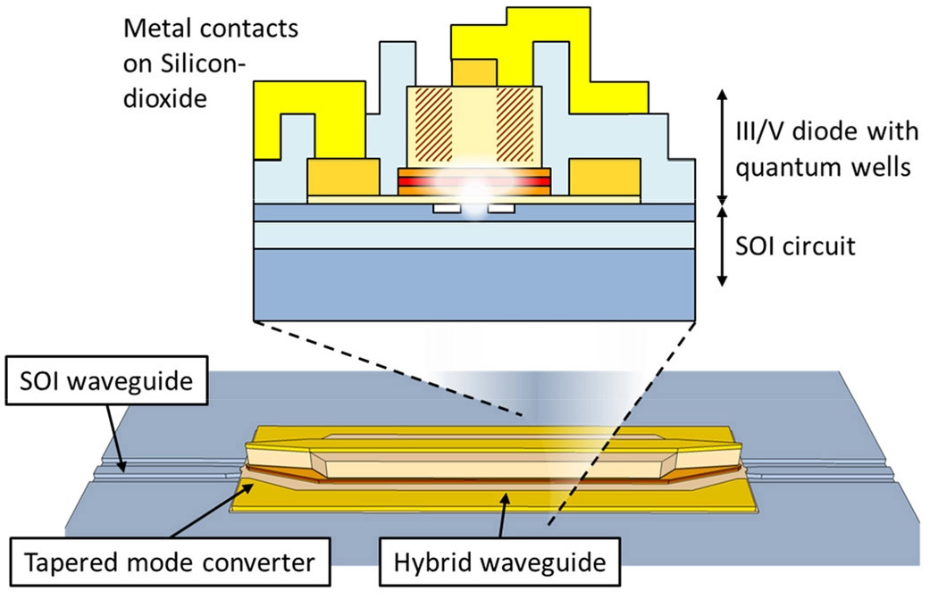
Lasers provide the initial coherent light source. In silicon photonics, heterogeneous integration bonds III-V materials like InP onto silicon for efficient lasing. These on-chip lasers support continuous-wave operation and narrow linewidths essential for long-reach links.
Modulators imprint electrical data onto optical carriers. Common types use carrier depletion in pn junctions or electro-absorption effects. They achieve high speeds over 100 Gb/s with low drive voltages, crucial for energy-efficient transmission.
Photodetectors complete the signal chain by turning light into electrical currents. Germanium-based designs integrate well with silicon waveguides, offering high responsivity and bandwidth. This enables sensitive reception even at faint signal levels.
Passive parts direct and manage light without external power. You rely on them for efficient routing in complex circuits.
Waveguides form the backbone for light propagation. Silicon strip or rib designs offer losses below 1 dB/cm. They connect all components reliably across the chip.
These devices combine or separate different wavelengths. Arrayed waveguide gratings or ring resonators enable dense wavelength-division multiplexing. This boosts bandwidth without adding fibers.
Grating couplers link chips to external fibers efficiently. Directional couplers and multimode interferometers split or combine signals precisely. They ensure low-loss transitions in multi-port designs.
Various material platforms suit different needs. You choose based on required active functions, cost, and scale.
Silicon photonics dominates due to CMOS compatibility and large wafer sizes. It excels in passive components and integration density. However, it requires hybrid approaches for lasers and amplifiers.
Indium phosphide supports monolithic integration of lasers, modulators, and detectors. Direct bandgap enables efficient light generation and detection. This makes it strong for transmitters needing high output power.
Hybrid methods bond InP actives onto silicon passives. You get low-loss waveguides plus native gain elements. This approach balances performance and manufacturing scale effectively.
Photonic chips power critical systems today. You see rapid adoption where speed and efficiency matter most.
Hyperscale facilities require terabit-scale links. Optical modules with integrated chips cut power and space needs. This supports growing AI workloads efficiently.
Massive GPU farms need low-latency interconnects. Co-packaged optics bring light close to processors. They reduce energy per bit dramatically.
LiDAR and precision sensors benefit from compact photonics. Integrated detectors and sources enable reliable operation in harsh environments.
You need suppliers who deliver ready-to-deploy technology. DEEPETCH focuses on high-speed solutions backed by strong R&D.
Their 400G to 800G transceivers incorporate advanced photonic components. Options include OSFP and QSFP-DD form factors with multiple reaches. These support Ethernet and InfiniBand protocols reliably.
Active development targets 1.6T and beyond. Integration of efficient modulators and detectors prepares for future demands. This keeps your infrastructure future-proof.
Tailored designs adapt to specific applications. Services cover full-series active optical cables and liquid-cooled modules. You receive optimized solutions quickly.
Select components that match your performance goals. Strong integration of actives and passives ensures long-term reliability and efficiency in demanding setups.
Q1: What makes SOI the preferred platform for photonic chips?
A: High index contrast enables compact designs and low losses, while CMOS compatibility reduces costs.
Q2: Why integrate lasers heterogeneously in silicon photonics?
A: Silicon lacks direct bandgap for efficient lasing, so III-V materials provide necessary gain.
Q3: How do passive components improve chip efficiency?
A: Low-loss waveguides and multiplexers maximize bandwidth without added power.
Q4: Which platform suits applications needing native light sources?
A: InP excels with monolithic lasers and amplifiers for high-power needs.
Q5: What drives hybrid integration adoption?
A: It combines silicon’s scale with InP’s active performance for balanced solutions.

The DE-CW-1310 DFB EPI wafer, a high-performance epitaxial structure designed for distributed feedback (DFB) lasers operating at 1310 nm....

Ceramic thin-filmvacuum sensor Optical gas massflowmeter Liquid mass flowmeter Force sensor MEMS...

Photoelectric sensing chip Light source chips Optical transmission and modulationchips Optical detection and receptionchips...

Using a“Detach Core”which has two-layers carrier foil structure on the surface as a core, and forming...

Tenting process is a kind of subtractive process, the process as follows: Laminating photosensitive film...

Modified Semi-Added Process abbreviated as mSAP, which can be used on the core or build-up layers, pattern...

Semi-Added Process abbreviated as SAP, using on the build-up-layer pattern forming as follow:First depositing...

The product generally adopts the pressing lamination process of semi-curing sheets , and line formation...

The products generally adopt the Build-up Film Lamination process, and the circuit formation uses the...

Equipment features: 1. Non-destructive precision testing Micrometer-level probe contact technology...