Data needs are reaching boundaries that conventional equipment cannot surpass any longer. Consider the rapid shift in data centers from 10G to 800G. This shows the sector is competing against natural barriers. You probably feel the demand for parts that deliver reduced delay and greater capacity without exceeding energy limits. Advancing to 6G demands going past ordinary silicon. It involves examining unique substances and combination methods. These were once viewed as specialized but now serve as key elements for thriving in the elevated-frequency period.

The path of the transceiver involves smaller sizes and larger capabilities. Initial data connections used straightforward electrical transmission and basic light changes. These suited the web from two decades past. Yet, as you advance to a 6G setting, emphasis has changed from merely transferring data to doing so at terahertz levels. This change requires a complete reassessment of signal paths across a circuit board. It also considers the heat a lone unit can manage effectively.
Early on, systems used SFP modules that achieved only basic gigabit rates. These depended on common silicon and simple laser diodes. As demands grew to 400G and 800G eras, issues with copper and standard fiber became obvious. Consequently, engineers had to seek alternatives to maintain progress.
The move to 6G represents far more than a minor upgrade from 5G. It brings in terahertz (THz) waves. Therefore, equipment must manage frequencies where typical PCB substances absorb signals excessively. This absorption occurs before the signal arrives at its target. As a result, new designs become necessary for reliable transmission.
Silicon performs well, but it faces constraints, particularly for rapid electron movement. When sending high-frequency signals via standard bases, power dissipation turns problematic. This issue affects those aiming for steady connections over extended ranges. Thus, alternative options gain importance for sustained performance.
To address these issues, the field is adopting compound semiconductors. If maintaining signal quality at 6G rates matters, consider substances like Indium Phosphide (InP). These offer quick electron speed and broad bandgap for fast changes and effective light output. It proves remarkable how changing the core substance can make 1.6T rates seem practical instead of mere tests.
InP excels due to its support for elevated frequency tasks over gallium arsenide or silicon. It delivers improved results in light sources and light detectors. For this reason, it forms the foundation for upcoming high-speed optical units. Such advantages ensure better overall system efficiency.
As parts shrink, heat generation increases. You may find it useful that DEEPETCH, a focused supplier started in 2019, addresses this directly. They have expanded output of 800G transceivers with fresh liquid cooling methods to prevent chip slowdowns in intense AI tasks. Their knowledge covers IDM approaches and tailored EMS offerings. This positions them as a reliable source for durable hardware that withstands stress without failure. In addition, their solutions support demanding applications effectively.
Combining InP with current CMOS methods represents a major goal in transceiver development. This mixed strategy preserves silicon’s affordability while adding the speed of compound materials. As a result, it balances cost and performance for practical use. Therefore, it aids in advancing network capabilities.
Substances form just part of the solution. The way you enclose them holds equal weight. High-frequency signals react strongly to their travel route. If the path, or base, proves uneven or extended, the signal degrades. For this reason, sophisticated packaging has evolved from a mere assembly stage to a central aspect of electrical planning.
You likely know of ABF substrate from advanced processors. Now, it plays a crucial role in 6G transceivers as well. This resin film enables very detailed circuit layouts. Such precision proves vital when fitting countless connections into limited areas. Consequently, it supports denser designs without loss.
Standard bases include a heavy central layer, but the Coreless Process eliminates it. This action shortens the signal’s vertical route through connections. The decreased length leads to lower resistance and stronger operation for fast data paths. Thus, it enhances transmission quality significantly.

In areas like MEMS and detectors, thin film methods build layers at atomic scale. For transceivers, this approach creates accurate barriers and superior separation between powerful parts and delicate routes. As such, it improves overall reliability and function. In turn, it meets the needs of complex systems.
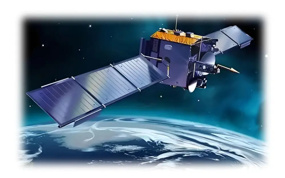
The 6G outlook features constant access, so transceiver methods must function in orbit as reliably as in controlled server rooms. Satellite links and sensing setups demand Transmit/Receive (TR) units that endure radiation and wide temperature changes. Here, the focus extends past velocity to complete resilience.
In orbit, repairs involve no on-site fixes for faulty units. Designs for flight must consider disruptions from space particles, like Single Event Upsets. This requires chip-level protections. Therefore, such measures ensure long-term operation in harsh conditions.
TR modules serve as the core of directed antenna arrays. These parts demand high integration and beam steering abilities. Such features let a satellite direct signals precisely to ground points without mechanical shifts. As a result, they enable efficient global coverage.
Substances like InP and ceramic enclosures assist greatly. Yet, the layout itself needs backup elements. In this domain, partial solutions fall short, and each trace length demands precise calculation for peak steadiness. Consequently, this approach guarantees robust performance.
Advancements occur rapidly, so ready-made components often lag by the launch of your initiative. This situation highlights the value of bespoke Electronic Manufacturing Services (EMS). A collaborator familiar with PCBA planning for 6G and flight applications speeds the path from initial model to operational part.
Designs must adapt to varying scales. This applies whether producing limited test 6G panels or large volumes of 800G units. The fabrication must accommodate strict limits and intricate layers. Thus, flexibility proves essential for diverse projects.
Initial 6G equipment frequently uses unusual bases like glass or specific resins. An expert EMS group guides selections before full commitment. This guidance prevents costly errors in later stages. As such, it streamlines development effectively.
Testing ranges from shake trials for aerial vehicles to heat simulations for orbit craft. This stage distinguishes effective from inadequate designs. Seek approvals like IATF 16949 or ISO 9001 to confirm shared quality standards. If seeking details on parts or stock, review the chips in stock for suitable high-frequency options in your upcoming assembly. In addition, these resources aid informed decisions.
Transitioning from basic data paths to 6G presents a significant challenge, yet it offers chances to guide the field. By emphasizing substances like Indium Phosphide and using methods such as Coreless and ABF substrates, you can overcome silicon’s constraints. Whether for ground-based servers or orbital networks, selecting gear built for tomorrow’s frequency demands ensures lasting success.
Q1: Why is Indium Phosphide better than Silicon for 6G?
A: InP has much higher electron mobility and can operate at terahertz frequencies where silicon starts to lose signal efficiency and generate too much heat.
Q2: What is the main advantage of a Coreless Process in transceivers?
A: It removes the thick center core of the substrate, which shortens the signal path, reduces impedance, and allows for much thinner and lighter high-speed modules.
Q3: Can these high-speed modules be used in satellites?
A: Yes, but they require specific TR (Transmit/Receive) chip designs that are radiation-hardened and tested for the extreme temperature cycles found in space environments.
Q4: How does ABF substrate help with 800G or 1.6T speeds?
A: ABF allows for incredibly fine-pitch circuit patterns, which are necessary to manage the high density of signals required for 800G and future 1.6T optical modules.
Q5: Do 6G transceivers require special cooling?
A: Often yes, especially in dense AI clusters. Innovations like liquid-cooled transceivers are becoming necessary to manage the thermal output of high-speed chips without sacrificing performance.

The DE-CW-1310 DFB EPI wafer, a high-performance epitaxial structure designed for distributed feedback (DFB) lasers operating at 1310 nm....

Ceramic thin-filmvacuum sensor Optical gas massflowmeter Liquid mass flowmeter Force sensor MEMS...

Photoelectric sensing chip Light source chips Optical transmission and modulationchips Optical detection and receptionchips...

Using a“Detach Core”which has two-layers carrier foil structure on the surface as a core, and forming...

Tenting process is a kind of subtractive process, the process as follows: Laminating photosensitive film...

Modified Semi-Added Process abbreviated as mSAP, which can be used on the core or build-up layers, pattern...

Semi-Added Process abbreviated as SAP, using on the build-up-layer pattern forming as follow:First depositing...

The product generally adopts the pressing lamination process of semi-curing sheets , and line formation...

The products generally adopt the Build-up Film Lamination process, and the circuit formation uses the...

Equipment features: 1. Non-destructive precision testing Micrometer-level probe contact technology...