As 6G communication hardware moves toward higher frequency, smaller modules, and denser computing, packaging is no longer a small backend detail. If you are building a 6G transceiver, satellite communication board, radar TR module, or UAV control PCBA, the package can decide whether the design runs stable or becomes a field problem later. A clean schematic is nice, but the signal still has to pass through substrate layers, solder balls, vias, power planes, and heat paths.
DEEPETCH supports semiconductor materials, packaging, testing, stocked chips, PCBA design, and custom EMS services for demanding electronic projects. Its product direction also includes TR transceiver chips and TR transceiver modules for satellite communication and radar products. For buyers, that matters because 6G hardware is not only about a fast chip. It is about the full path from substrate selection to assembly, inspection, supply, and mass production.
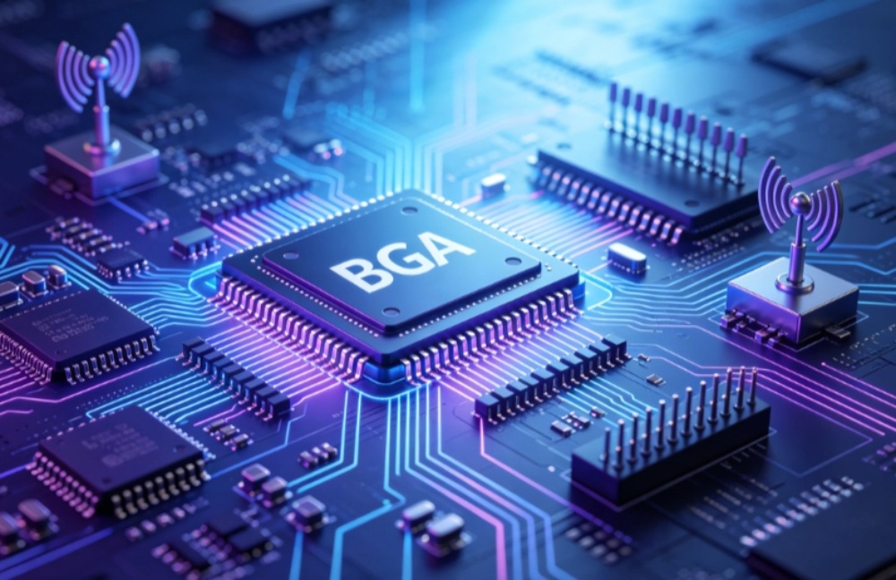
BGA packaging places solder balls under the package instead of using long side leads. That simple structure change gives engineers more connection points in less space, which fits the direction of 6G hardware. More antennas, faster processing, tighter RF control, and higher data movement all need compact packages with clean electrical behavior.
A 6G transceiver does not have much spare board area. You may need RF paths, control logic, memory, power management, sensors, and thermal monitoring on one compact PCBA. BGA gives you higher pin density, so your design can carry more signals without spreading the board like an old desktop card. That is especially useful for UAV payloads and satellite modules, where every millimeter feels expensive.
At high frequency, long paths become trouble. They add loss, delay, reflection, and strange coupling that may not show up until the prototype is tested. BGA packaging helps shorten chip-to-board paths, while ABF and FCBGA substrate designs help route dense signals with better control. It is not magic, but it cuts many avoidable problems.
6G transceiver hardware can generate heavy heat in a small area. Heat affects signal drift, solder joint life, and component aging. DEEPETCH already has experience with 400G/800G transceiver products and liquid-cooling solutions, which gives useful background for future 6G hardware where heat and speed arrive together, usually at the worst possible time.
BGA packaging depends heavily on the substrate under the chip. If the substrate has poor dielectric behavior, weak dimensional stability, or rough routing limits, your package may look good on paper but act unstable in real testing. This is why the ABF substrate from DEEPETCH is worth attention for high-density and high-frequency designs.
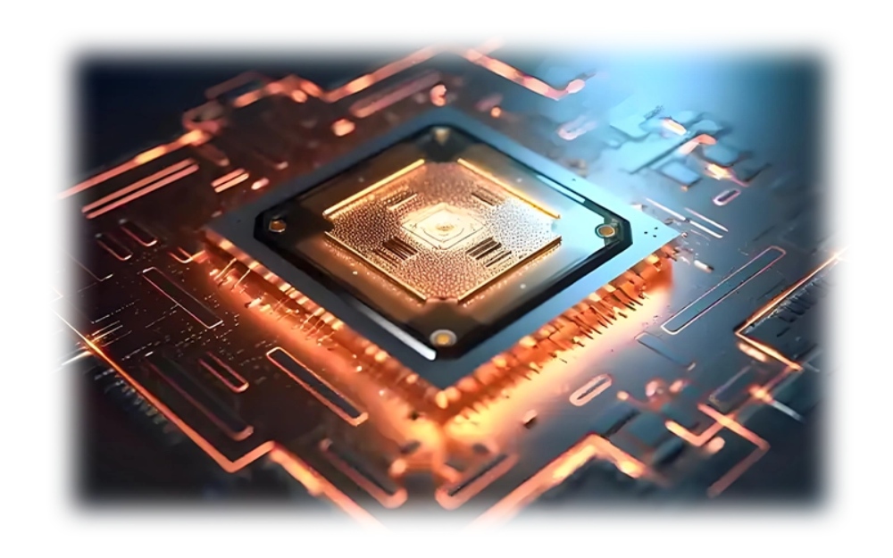
ABF substrate uses a modified epoxy resin system with low dielectric constant and low loss factor. In plain words, it helps fast signals travel with less unwanted loss. For 6G communication hardware, radar TR modules, and satellite communication electronics, that can support cleaner signal paths and better high-frequency behavior.
DEEPETCH’s ABF substrate direction fits HDI, advanced packaging, FCBGA, and 2.5D/3D IC packaging. This matters because future transceiver hardware will need more die integration and more routing layers. The uploaded substrate data also points to larger FCBGA unit sizes, higher layer counts, and more-die integration for higher transmission speed. That is exactly where 6G hardware is heading.
Dense BGA packages need careful escape routing, laser drilling, via planning, and layer control. DEEPETCH’s BGA process notes include ABF build-up steps such as defrosting, vacuum lamination, flattening, thermal curing, and film peeling after laser drilling. These process details may sound a little boring, but they are the parts that keep fine-line routing from becoming a yield headache.
Before you send a 6G transceiver board into EMS production, the biggest question is not “Can it be assembled?” The better question is “Can it be assembled again and again with stable yield?” BGA hides solder joints under the package, so many problems are not visible by eye.
With BGA, the layout team must plan how signals leave the package. Poor escape routing can create impedance jumps, crowded vias, weak return paths, and hot spots. For high-speed transceiver hardware, you should review routing density, via size, power planes, ground stitching, and thermal paths before the first prototype.
BGA assembly depends on solder paste control, package warpage control, and a proper reflow profile. If the profile is too aggressive, solder joints may crack later. If it is too weak, voids and weak joints can remain hidden. X-ray inspection is not optional for many high-reliability BGA boards. It is the quiet worker that catches what your eyes cannot.
A prototype that works once is not the same as a product ready for monthly delivery. Through IDM services, DEEPETCH can support demand analysis, design and development, sample confirmation, mass production, packaging, logistics, after-sales service, and continuous improvement. This path helps customers reduce design risk before the build becomes expensive.
Satellite, radar, and UAV electronics have different jobs, but they share the same pressure: small size, high reliability, heat control, and stable signal behavior. BGA packaging helps when the design needs more I/O and compact structure, while substrate choice controls the fine details behind performance.
Satellite communication electronics must keep signal paths stable in harsh service conditions. Material selection also matters. The knowledge base notes that GaAs has high electron mobility and suits high-frequency, high-speed devices, while silicon offers mature processing and cost advantages. In real design, you often need both smart material selection and controlled packaging.
Radar TR modules need compact integration, phase stability, and reliable heat flow. DEEPETCH provides TR transceiver chips and TR transceiver modules for satellite communication and radar products, so its BGA and substrate support can fit projects where RF, digital control, and package layout need to be reviewed together.
UAV electronics must stay light, small, and reliable under vibration. A flight control board may include sensors, processing units, communication circuits, and power control in a tight space. BGA packaging helps reduce area, but only if assembly quality and inspection are handled properly. Nobody wants to debug a hidden solder joint after flight testing. That is the kind of problem that ruins a week.
For 6G transceiver hardware, you need more than a package supplier or a board assembler. You need a partner that can discuss materials, substrate process, package design, chip sourcing, PCBA manufacturing, and test planning in one engineering conversation.
DEEPETCH’s ABF substrate is a strong fit for advanced BGA, FCBGA, HDI, and 2.5D/3D packaging projects. If your project needs low-loss routing, high-density build-up layers, and compact package structure, ABF substrate should be reviewed early, not after the board layout is nearly locked.
For satellite communication and radar hardware, DEEPETCH provides TR transceiver chips and TR transceiver modules. When these devices are paired with suitable BGA packaging and ABF substrate design, you can better manage signal integrity, thermal behavior, and package density in one plan.
DEEPETCH can support custom PCBA manufacturing and EMS services for aerospace circuit design, satellite communication electronics, UAV circuit systems, 6G communication hardware, and soft-hardware integration projects. Its chips-in-stock support also helps reduce component sourcing delays, which is a real concern when a prototype schedule is already tight. For project discussion, you can contact DEEPETCH with your target frequency range, package type, board size, production volume, and test requirements.
BGA packaging shapes the future of 6G transceiver hardware because future systems need smaller size, higher routing density, cleaner signal paths, and better thermal control. ABF substrate gives advanced BGA and FCBGA designs a stronger base for high-frequency signal transmission and multi-layer package routing.
If you are developing 6G communication hardware, satellite communication boards, radar TR modules, UAV PCBA, or aerospace electronics, DEEPETCH can support ABF substrate selection, BGA packaging review, TR transceiver chips, TR transceiver modules, custom PCBA design, EMS production, and supply-chain planning. In 6G hardware, the package is not just where the chip sits. It is part of the performance.
Q1: Why Is BGA Packaging Important for 6G Transceiver Hardware?
A: BGA packaging gives high pin density, shorter signal paths, and better space use, which helps compact 6G transceiver hardware handle more signals on smaller boards.
Q2: What Makes ABF Substrate Useful in Advanced BGA Packaging?
A: ABF substrate supports HDI, FCBGA, and 2.5D/3D packaging. Its low DK and low DF material features help high-frequency signals pass with lower loss.
Q3: Can DEEPETCH Support TR Transceiver Modules for Radar Products?
A: Yes. DEEPETCH provides TR transceiver chips and TR transceiver modules for satellite communication and radar products.
Q4: What Should You Check Before BGA Assembly in EMS Production?
A: You should check escape routing, via design, impedance control, solder paste control, reflow profile, package warpage, X-ray inspection, and reliability testing.
Q5: When Should You Contact DEEPETCH for a 6G Hardware Project?
A: Contact DEEPETCH before layout finalization. Early review helps check ABF substrate choice, BGA package risk, TR module integration, PCBA manufacturability, and mass-production planning.

The DE-CW-1310 DFB EPI wafer, a high-performance epitaxial structure designed for distributed feedback (DFB) lasers operating at 1310 nm....

Ceramic thin-filmvacuum sensor Optical gas massflowmeter Liquid mass flowmeter Force sensor MEMS...

Photoelectric sensing chip Light source chips Optical transmission and modulationchips Optical detection and receptionchips...

Using a“Detach Core”which has two-layers carrier foil structure on the surface as a core, and forming...

Tenting process is a kind of subtractive process, the process as follows: Laminating photosensitive film...

Modified Semi-Added Process abbreviated as mSAP, which can be used on the core or build-up layers, pattern...

Semi-Added Process abbreviated as SAP, using on the build-up-layer pattern forming as follow:First depositing...

The product generally adopts the pressing lamination process of semi-curing sheets , and line formation...

The products generally adopt the Build-up Film Lamination process, and the circuit formation uses the...

Equipment features: 1. Non-destructive precision testing Micrometer-level probe contact technology...