
SOP and SOIC packages can look almost identical on a component list, yet a small dimensional mismatch can force a PCB respin. The safest rule is simple: do not select a land pattern from the package name, pin count, or 1.27 mm pitch alone. Check the exact package drawing for body width, lead span, lead length, height, and recommended PCB land pattern before releasing the board.
For engineering teams working through package selection, DEEPETCH provides semiconductor packaging, ceramic package, IC substrate, and engineering support. The practical goal is to match package geometry to assembly conditions early enough to avoid poor solder fillets, lifted leads, thermal problems, or incompatible footprints during prototype and volume production.
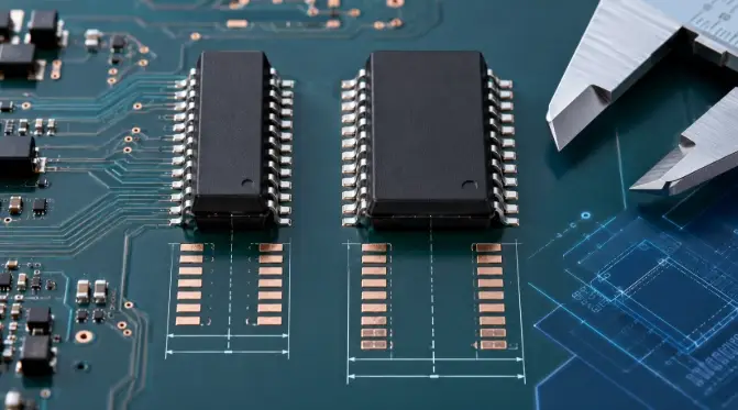
Both SOP and SOIC are surface-mount integrated-circuit packages with gull-wing leads on two opposite sides. The confusion comes from naming practice: SOP is often used as a broad small-outline package family term, while SOIC usually refers to a more specifically defined small-outline integrated-circuit format. In supplier catalogs, however, SOP, SOP-J, SOIC, wide SOIC, and regional package codes can overlap in appearance. That is why package identification should always start from the mechanical drawing rather than the label alone.
Many SOIC outlines are associated with JEDEC conventions, while many SOP variants found in Japanese and Asian supplier catalogs follow JEITA/EIAJ-style naming or supplier-specific drawings. The important engineering point is not the regional label itself, but the controlled dimensions behind it. Two 8-pin packages can share the same nominal pitch and still require different PCB pads because the body and lead span are different.
For a broader background on the package family, see SOP vs SOIC Packaging Types.
| Comparison Item | SOIC | SOP | Engineering Meaning |
| Mounting style | Surface mount, gull-wing leads | Surface mount, gull-wing leads | Assembly method can look identical |
| Common pitch | 1.27 mm is common | 1.27 mm is common; other SOP-family pitches also exist | Same pitch does not prove footprint compatibility |
| Typical body style | Narrow and wide variants | Multiple regional/supplier variants | Body and lead-span dimensions must be checked |
| Common lead counts | 8, 14, 16, 20, 24, 28 and others | 8, 14, 16, 20, 24, 28 and others | Pin count alone is not a package identifier |
| Standards / naming | Often associated with JEDEC outlines | Often associated with JEITA/EIAJ or supplier SOP codes | Use the drawing, not only the package name |
| Typical applications | Analog, interface, logic, memory, power-management ICs | Analog, mixed-signal, optoelectronic, industrial and specialty ICs | Application does not determine footprint |
Dimension comparison is where most design errors occur. A narrow SOIC commonly uses an approximately 3.8-3.9 mm body width, while wider SOP-style 8-pin outlines around 4.9-5.3 mm are also common in supplier catalogs. Those figures are useful for recognizing the package family, but they are not universal limits. The final PCB footprint must follow the exact component datasheet.
| Dimension | What to Check | Why It Matters | Safe Design Rule |
| Lead pitch | Center-to-center spacing between adjacent leads | Controls pad spacing and solder-mask clearance | Do not assume identical body geometry because pitch matches |
| Body width | Plastic or ceramic body width | Changes lead reach and package courtyard | Verify the drawing, especially for narrow vs wider variants |
| Body length | Package length along the pin rows | Affects courtyard and nearby component clearance | Use the exact package code |
| Overall lead span | Distance from lead tip to lead tip across the package | Directly affects where pads must sit | Critical for interchangeability checks |
| Lead width / length | Gull-wing lead geometry | Affects pad width, heel and toe fillets | Follow land-pattern guidance |
| Package height | Maximum seated height | Affects enclosure and stacked-board clearance | Check mechanical constraints |
| Exposed pad, if present | Center thermal/ground pad size | Changes stencil, thermal via and solder-volume design | Treat exposed-pad versions as a separate footprint |
A common sourcing mistake is to compare two parts described as “8-pin, 1.27 mm pitch” and assume they can share a footprint. That ignores overall lead span, body width, lead length, and manufacturer tolerances. A component may electrically replace another part yet still be mechanically incompatible with the existing PCB land pattern.
Sometimes, but never by assumption. SOP and SOIC are interchangeable only when the exact mechanical drawings and recommended land patterns are compatible. The fact that two parts have the same pin count, electrical pinout, or 1.27 mm pitch is not sufficient.
If any critical dimension differs enough to reduce heel or toe solder fillet, push the lead toward the edge of the pad, or violate the courtyard, the packages should be treated as different footprints.
The most common mistake is placing a wider SOP-style package onto a land pattern created for a narrow SOIC because both are labeled “8-pin.” The leads may land too far toward the outside or inside of the pads, leaving weak heel fillets or inconsistent solder volume. The reverse substitution can also create oversized pads, excess solder, or inspection uncertainty. The correct conclusion is not “SOP and SOIC can never be swapped,” but “compatibility must be proven from the drawings.”
Once the exact package is identified, the footprint should be designed around solder-joint goals and the assembly process. IPC-7351 land-pattern principles are useful for heel, toe, side, courtyard, and density-level decisions, but the component manufacturer’s package drawing remains the starting point.
The pad must provide enough heel and toe extension for a repeatable gull-wing solder joint without creating unnecessary solder volume. Pads that are too short can reduce mechanical anchoring, while pads that are too wide or closely spaced can increase bridging risk. Solder-mask web, stencil aperture, copper finish, paste type, and reflow profile should be reviewed together rather than as independent dimensions.
Some SOIC-family devices include an exposed center pad for heat transfer or grounding. That version requires a dedicated thermal-pad pattern, stencil segmentation, and often thermal vias to internal or backside copper. It should not share a footprint with a standard non-exposed-pad package unless the datasheet explicitly supports it. Lead coplanarity also matters because lifted gull-wing leads may not wet correctly during reflow.
| Mistake | Likely Result | Better Practice |
| Selecting the footprint from “SOP-8” or “SOIC-8” text only | Wrong pad spacing or courtyard | Use the full package code and drawing |
| Assuming equal 1.27 mm pitch means equal footprint | Weak heel fillets or shifted lead position | Compare overall lead span and lead geometry |
| Ignoring exposed-pad versions | Poor thermal or ground connection | Create a separate exposed-pad footprint |
| Copying a generic library footprint without verification | Assembly variation across suppliers | Compare library data to the actual datasheet |
| Ignoring package height | Mechanical collision in enclosure or stacked PCB | Include maximum seated height in mechanical review |
There is no strict application boundary between SOP and SOIC. Both appear in analog, mixed-signal, interface, sensor, memory, logic, and power-management products. SOIC is common in standardized component libraries, while SOP naming is widely used across supplier-specific and regional package families. For procurement, application should be treated as context, not as evidence that one footprint will fit another.
If the project requires hermetic sealing, wider temperature capability, low dielectric loss, or stronger environmental protection, a standard plastic outline may no longer be the best choice. DEEPETCH’s Ceramic SOP product line uses glass or metal-solder sealing, lists helium leakage below 1 × 10⁻⁸ atm·cc³/s, supports 0.65 mm, 0.8 mm, and 1.27 mm pin spacing options, and provides wide-temperature package options for high-reliability electronics.

SOP and SOIC are efficient when the required I/O count, lead pitch, thermal load, and board area fit a leaded package. If the design needs much higher I/O density, finer routing, multi-die integration, or shorter high-speed interconnects, a custom substrate architecture may be more appropriate. DEEPETCH Custom IC Substrates use ABF build-up structures for high-density routing and should be evaluated as a different packaging path rather than as a direct SOP/SOIC substitute.
The fastest way to prevent footprint errors is to convert the package decision into a short release checklist before Gerber output, alternate-part approval, or purchase-order release.
When a datasheet uses ambiguous SOP/SOIC naming, the package drawing should be reviewed before the footprint is frozen. Engineering teams can contact DEEPETCH to discuss package dimensions, ceramic packaging options, substrate requirements, and custom assembly constraints before prototype release.
Both are gull-wing surface-mount package families, but naming conventions and mechanical outlines can differ. The practical difference for PCB design is the exact body width, lead span, lead dimensions, height, and recommended land pattern shown in the component drawing.
Not necessarily. They may share eight leads and a 1.27 mm pitch, yet still have different body or lead-span dimensions. Always compare the two package drawings before using the same footprint.
A: Only if the mechanical dimensions and land-pattern requirements are compatible. Do not approve the substitution from pin count or pitch alone. Check lead span, pad position, heel and toe fillets, courtyard, and the manufacturer’s recommended footprint.
Check pin pitch, body width, body length, overall lead span, lead width, lead length, package height, and any exposed thermal pad. The full package code should match the PCB library entry.
Ceramic SOP is appropriate when the application needs hermetic sealing, wider temperature capability, stronger environmental protection, or specialized electrical and thermal performance that standard plastic packaging cannot provide.
Yes. If the site template supports it, the visible FAQ questions can also be implemented with valid FAQPage structured data so search engines can parse the question-and-answer structure consistently.

Diamond-Copper Thermally Conductive Composite. High thermal conductivity, tunable CTE, robust.

The DE-CW-1310 DFB EPI wafer, a high-performance epitaxial structure designed for distributed feedback (DFB) lasers operating at 1310 nm....

Ceramic thin-filmvacuum sensor Optical gas massflowmeter Liquid mass flowmeter Force sensor MEMS...

Photoelectric sensing chip Light source chips Optical transmission and modulationchips Optical detection and receptionchips...

Using a“Detach Core”which has two-layers carrier foil structure on the surface as a core, and forming...

Tenting process is a kind of subtractive process, the process as follows: Laminating photosensitive film...

Modified Semi-Added Process abbreviated as mSAP, which can be used on the core or build-up layers, pattern...

Semi-Added Process abbreviated as SAP, using on the build-up-layer pattern forming as follow:First depositing...

The product generally adopts the pressing lamination process of semi-curing sheets , and line formation...

The products generally adopt the Build-up Film Lamination process, and the circuit formation uses the...