
The practical answer to flip chip vs wire bonding starts with the die drawing, not the package label. Choose flip chip when the connection layout and package requirements justify a bumped, face-down attachment. Choose wire bonding when accessible pads, available space and a qualified bonding process meet the electrical and reliability targets. Neither route is a universal upgrade; the decision has to include the die, carrier, assembly process and test plan.
For a package engineer, the first useful document is the pad or bump map. For a buyer, it is that same map paired with a feasible assembly proposal and a clear test scope. Comparing a bumping quote with a wire-bond assembly quote before those boundaries are aligned can make the cheaper option appear obvious while important work remains unpriced.
This guide covers connection layout, electrical and thermal paths, assembly controls, qualification, total cost, and the information to send for a packaging review.

In conventional wire bonding, the die is attached with its bonding surface accessible. Fine wires connect the die pads to leads or substrate bond fingers. The wire loops take up space, and their geometry is part of the electrical and mechanical design. Many familiar leadframe and laminate packages use this approach.
In flip chip assembly, conductive bumps or pillars on the die connect to matching carrier pads with the active side facing the carrier. Connections can be distributed across the die surface, subject to the actual die design. This arrangement can shorten the die-to-carrier path and ease some perimeter-pad constraints. DEEPETCH’s FCBGA substrate page provides the relevant carrier context for an initial package discussion.
Do not confuse the internal interconnect with the package’s board connection. A ball grid array describes the external solder-ball arrangement. A BGA package can use a wire-bonded die or a flip-chip die internally. Similarly, selecting a QFN outline does not, by itself, define every detail of the internal assembly.
DEEPETCH’s packaging documentation lists wire-bond BGA, several flip-chip formats and hybrid constructions. These are options for a technical discussion, not an assurance that every listed format is available for any die. Ask for a project-specific process and package review.
| Question | Wire bonding | Flip chip |
| How are die pads reached | Wires connect accessible pads to leads or bond fingers | Bumps or pillars connect to matching carrier pads |
| What occupies package space | Bond fingers, wire loops and clearances | Bump field, routing escape and assembly clearances |
| What must be modeled electrically | Wires, return paths and package routing | Bumps, transitions, return paths and package routing |
| What assembly work needs definition | Die attach, wire material, bonding and encapsulation | Bumping, alignment, joining and any underfill process |
| What makes a fair cost comparison | Complete tested assembly scope | Complete tested assembly scope |
The table is a starting checklist. Package performance comes from the actual geometry and materials, not the heading in the right-hand column.
For wire bonding, inspect pad locations, pad opening, metallurgy and the permitted bonding conditions. Confirm that the proposed wire route can reach the bond finger without interfering with neighboring wires or package features. A die intended for perimeter bonding may fit a familiar assembly flow without changing its pad arrangement.
For a flip chip proposal, establish whether the incoming wafer or die is already bumped. If it is not, the quote needs to identify responsibility for under-bump metallization, bumping and any redistribution work. Ask who approves the bump map and how the die supplier’s requirements are carried into the assembly drawing.
Do not compare I/O count in isolation. A perimeter-pad die and an area-array die can present different constraints even at the same count. The power and ground locations matter too. A design that fits all signal connections but leaves an impractical return path has not completed the interconnect review.
There is no universal pin count above which wire bonding stops being useful. The boundary depends on die dimensions, pad layout, package footprint and qualified process rules. Ask the assembly partner to show the proposed layout before accepting a general statement that the die “needs flip chip.”
A dense bump map may increase the demands on substrate escape routing. Review the line/space rules, via lands, layer count and alignment allowances alongside the assembly proposal. DEEPETCH’s FCBGA substrates are relevant to that discussion. A substrate capability figure is not, on its own, an assembly capability figure.
For a smaller package, DEEPETCH also provides FCCSP substrate information. The appropriate carrier still depends on the actual bump arrangement and electrical requirements. Keep the carrier drawing and assembly drawing under coordinated revision control; otherwise, a change approved by one supplier can invalidate the other’s assumptions.
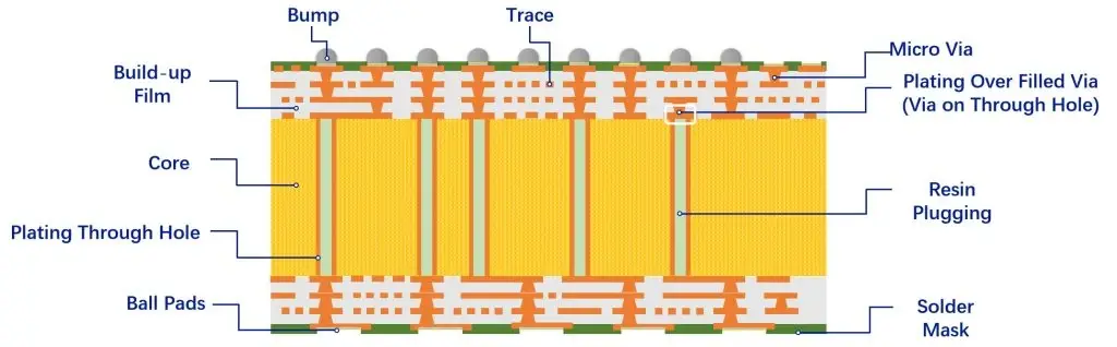
A shorter die connection can be valuable for a demanding electrical design, but the comparison should extend beyond the wire or bump. Include the package trace, via transitions, reference planes and board interface in the model. The interconnect choice should improve the path that is limiting the product, rather than a geometry that is easy to describe in a brochure.
For a wire-bonded candidate, review loop length and height, wire spacing and power or ground connections. For the bumped candidate, review the bump distribution and how the substrate carries current away from it. Ask for the model assumptions as well as the result. Different boundary conditions can make two simulation plots look more comparable than they are.
Wire material is another decision, not a fixed feature of wire bonding. Gold, copper and other wire systems require appropriate process and material compatibility. DEEPETCH’s packaging service information can be used to frame a project-specific discussion of assembly scope and process compatibility. A lower-cost wire should not be substituted without considering the die-pad structure and qualified bonding process.
Avoid attaching a universal speed limit to either technology. If a wire-bonded design meets the electrical target with acceptable margin, the case for changing it must come from another requirement or a demonstrated improvement. If it fails, identify the limiting part of the path before choosing the remedy.
Flip chip can leave the die backside accessible for a thermal interface or lid, depending on the package construction. That can be useful, but the result depends on what is attached to that backside and where the heat goes afterward. A lid without an adequate downstream cooling path does not resolve a system-level thermal problem.
A wire-bonded package can conduct heat through the die attach and an exposed pad or another designed path. It should not be rejected merely because wires are visible in its cross-section. Compare the proposed assemblies at the same dissipated power and boundary conditions, with the intended board and cooling arrangement represented.
Ask the thermal reviewer to identify the assumptions most likely to change the answer: die power distribution, interface materials, board construction and external cooling. Record these with the result. A thermal number from a different package or test board is not a direct prediction for the new product.
For wire bonding, the review should cover die-attach quality, pad condition, wire geometry, bonding parameters and encapsulation. Agree on the relevant inspection and bond-strength tests with the assembly partner. The aim is to establish evidence for the actual die, wire and package combination.
For a flip chip route, review incoming bump condition, alignment, joint formation and package deformation during assembly. If underfill is part of the construction, define its material, application, cure and inspection requirements. Underfill fills the die-to-carrier gap and participates in the mechanical behavior of the assembly; it is not a generic checkbox that makes every package reliable.
Inspection must match the defect. Optical inspection is useful where the feature is visible, while hidden joints need suitable inspection and electrical evidence. Do not describe one inspection method as proof that every relevant failure mode has been excluded. Establish what each check can and cannot reveal.
The qualification plan should name the package construction, material set, test conditions and pass criteria. Depending on the intended use, the team may need to investigate moisture-related damage, delamination, interconnect fatigue or other failure mechanisms. Specify the applicable methods with the customer and assembly partner rather than inventing a universal test sequence.
A wire substitution, new underfill, revised substrate finish or different die thickness can change the qualified construction. Ask which changes trigger engineering review, additional testing or customer approval. This is particularly important when a quotation allows unspecified “equivalent” materials.
DEEPETCH’s technical documentation includes both flip-chip and die-attach/wire-bond processes. Use these as the starting scope for a discussion of the proposed assembly. Current tolerances, material compatibility and qualification coverage must be confirmed for the project, not inferred from a broad capability list.
Align the quote boundaries first. Does the price include wafer bumping, die preparation, substrate, die attach, interconnection, underfill or molding, final test and packing? Identify nonrecurring tooling and engineering charges separately. A route that arrives with bumped die should not be compared directly with one that includes bumping unless the missing cost is restored.
Yield affects the comparison because assembly consumes valuable die. As a simple hypothetical screen, a route costing 5 currency units per started assembly at 95% acceptance costs about 5.26 units per accepted assembly. A 6-unit route at 99% acceptance costs about 6.06 units. Neither number includes die value unless it is explicitly placed in the starting cost. These inputs illustrate the calculation and are not supplier quotations or reported production results.
Include qualification expense and schedule where the program requires a change of technology. For a stable design, moving from a known wire-bond flow may need more justification than a small theoretical electrical gain. For a new die whose connection layout cannot fit the planned package, the extra assembly work may be unavoidable. The commercial comparison should describe which situation applies.
Imagine a hypothetical controller with accessible perimeter pads, adequate package space and no unresolved electrical limitation in a qualified wire-bond proposal. The immediate task is to confirm the process, inspection and cost. Changing the interconnect simply to use a newer package label would create additional work without an identified requirement.
Now imagine a hypothetical high-I/O die designed around an area-array bump map. A flip chip route is a natural candidate, but the team still needs to prove substrate escape, joining conditions and the thermal arrangement. The bump map points toward an architecture; it does not complete the package design.
Hybrid packages can also be appropriate. DEEPETCH’s packaging documentation includes flip-chip-plus-wire-bond configurations; its FCCSP substrate page is a useful starting point when reviewing a compact carrier. Consider a hybrid only when the dies and package functions call for it, with a clear assembly sequence and qualification plan.
Provide the die drawing and pad or bump map first, then add the constraints needed to evaluate it:
Ask for a proposed interconnect layout, process flow, material list and exceptions to the requirements. Identify who owns each unresolved item, especially bumping, substrate design and final test. This makes the next discussion a design review instead of another exchange of general capability slides.
It can offer a shorter die-to-carrier connection, but product performance depends on the full electrical path. Compare the actual package geometries and their modeled or measured behavior. A wire-bonded package that meets the target should not be dismissed using a generic technology ranking.
Do not assume the same underfill requirement for every construction. The interconnect, die size, carrier and application affect the assembly decision. The package supplier should specify whether underfill is used and provide the corresponding process and qualification basis for that construction.
Yes. BGA identifies the external ball-grid connection, while wire bonding and flip chip identify internal die connections. Confirm the package cross-section before comparing proposals; the same broad package label can describe different internal interconnect arrangements and manufacturing scopes.
The flip chip vs wire bonding decision is ready when the pad map, electrical path, thermal design and qualified assembly proposal agree. Compare complete tested-package costs after that technical review. To discuss the available route with DEEPETCH, send the die and packaging requirements, including the information above and any constraints that cannot change.

The DE-CW-1310 DFB EPI wafer, a high-performance epitaxial structure designed for distributed feedback (DFB) lasers operating at 1310 nm....

Ceramic thin-filmvacuum sensor Optical gas massflowmeter Liquid mass flowmeter Force sensor MEMS...

Photoelectric sensing chip Light source chips Optical transmission and modulationchips Optical detection and receptionchips...

Using a“Detach Core”which has two-layers carrier foil structure on the surface as a core, and forming...

Tenting process is a kind of subtractive process, the process as follows: Laminating photosensitive film...

Modified Semi-Added Process abbreviated as mSAP, which can be used on the core or build-up layers, pattern...

Semi-Added Process abbreviated as SAP, using on the build-up-layer pattern forming as follow:First depositing...

The product generally adopts the pressing lamination process of semi-curing sheets , and line formation...

The products generally adopt the Build-up Film Lamination process, and the circuit formation uses the...
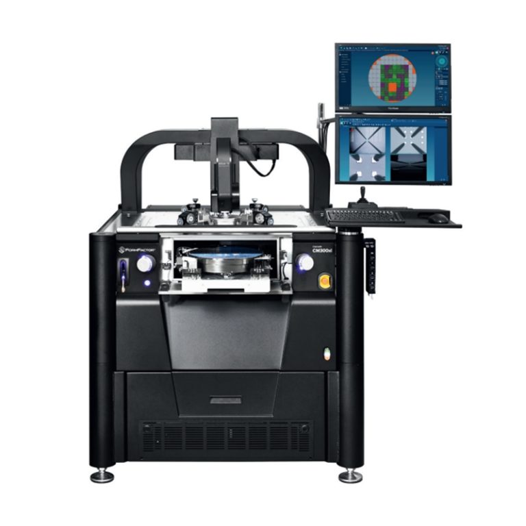
Equipment features: 1. Non-destructive precision testing Micrometer-level probe contact technology...