
An ABF substrate becomes a strong candidate when a package genuinely needs dense escape routing and several fine-line build-up layers. A BT substrate deserves evaluation when its qualified construction can route the die and meet the assembly requirements at an acceptable cost. The choice starts with the die, the interconnect and the finished stackup. A resin name alone cannot settle it; the actual design and yield target must decide.
For package designers and sourcing engineers, the difficult part is making two quotations comparable. One supplier may describe a build-up dielectric; another may quote a glass-reinforced laminate construction. Both may use the word substrate. Before comparing price, establish the exact stackup, process scope and yield assumptions each supplier intends to manufacture.
This guide covers material definitions, routing and stackup, electrical and mechanical checks, cost comparison, and the information needed for an RFQ.

ABF stands for Ajinomoto Build-up Film. It is an insulating film used in package substrates, not a finished circuit by itself. Copper wiring and vias are formed through subsequent manufacturing steps. DEEPETCH’s IC packaging substrate category provides the substrate context for this discussion. Even the instruction “use ABF” leaves the material specification incomplete, because the grade and finished stack still have to be named.
BT refers to bismaleimide triazine resin. In package-substrate discussions, the term often describes resin-based laminate and prepreg systems that may include glass reinforcement. The DEEPETCH BT resin product page is a useful starting point for the material discussion. The resin chemistry, reinforcement and laminate construction need to be identified together.
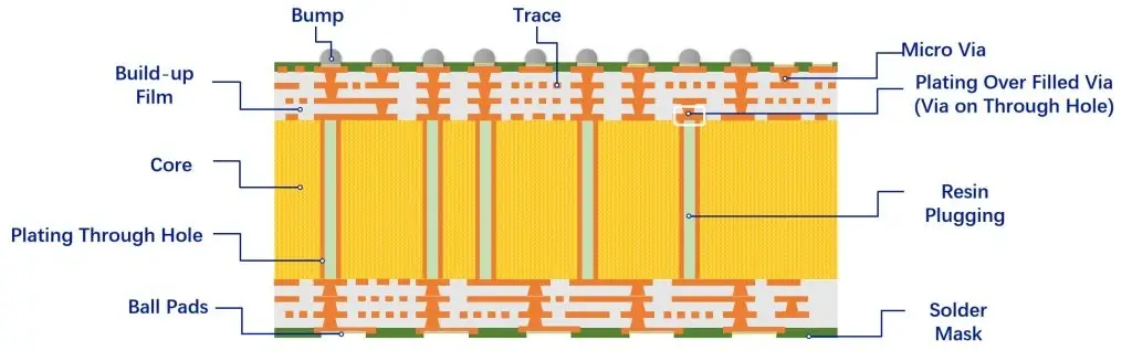
These terms do not always describe competing layers. A package can have one material system in its core and another in its outer build-up layers. Ask for a cross-section showing the core, dielectric layers, copper layers and via connections. Otherwise, “ABF versus BT” can become a comparison between different parts of the same structure.
The package label is a separate issue. FCBGA means flip-chip ball grid array and describes a packaging arrangement, not an exclusive resin choice. DEEPETCH’s FCBGA substrate range includes build-up processing and also discusses BT-based FCBGA capability. Do not assume that every FCBGA requires the same dielectric or layer count.
| Decision point | ABF build-up construction | BT-based construction |
| What must be specified | Film grade, core, build-up stack and process | Laminate grade, reinforcement, stack and process |
| Routing question | Can fine-line layers and microvias escape the bump map | Can the qualified line, via and layer rules route the package |
| Electrical check | Actual dielectric data and copper geometry | Actual dielectric data and copper geometry |
| Mechanical check | Full-stack warpage through assembly temperatures | Full-stack warpage through assembly temperatures |
| Purchasing basis | Accepted substrates and assembled-package yield | Accepted substrates and assembled-package yield |
There is deliberately no universal winner in the electrical or mechanical rows. Material families contain different grades, while the package adds copper, silicon and assembly materials. A useful comparison needs the proposed constructions, not a table of unrelated headline properties.
Start with the pad or bump map. Record the minimum pitch, I/O locations, power and ground distribution, keep-out regions and package outline. Then ask the substrate designer to show how the connections leave the die footprint. A large I/O count is useful context, but two dies with the same count may have very different escape problems.
The narrowest line and space matter only where they are needed. If one quote uses fine geometry everywhere and another restricts it to the escape region, they are not identical manufacturing proposals. Identify the critical area and ask whether wider traces can be used elsewhere. This makes the drawing more informative than a single minimum line/space number.
Vias consume routing space as well. Review the hole diameter, landing pad, registration allowance and whether stacked or staggered microvias are proposed. A smaller nominal hole does not automatically release usable routing channels if its land and registration requirements remain large. Ask for the actual design-rule set used in the routing study.
An ABF substrate often enters the discussion because build-up processing offers a route to dense interconnection. That is a reason to evaluate it, not permission to skip design-for-manufacture review. Confirm which geometry is qualified for the chosen construction and which figures are development targets.
Layer notation can be surprisingly ambiguous in an RFQ. In a common convention, 5+2+5 describes five build-up routing layers on each side of a two-layer core, giving twelve copper layers. The supplier should state its convention and provide a drawing; the notation alone is not a manufacturing specification.
DEEPETCH’s technical documentation contains a separate 14-layer FCBGA example with a 45 × 45 mm unit size and 15/15 μm minimum line/space, using an ABF GL-102 build-up layer. These are details of that documented example. They are not a claim that every size, layer count and minimum feature can be combined in a new order.
For a live project, request a stackup specific to the die. If the supplier adds layers during routing, revisit thickness, via structure and cost together. Adding copper layers may solve escape routing while creating a new assembly or mechanical constraint.
Do not select an IC substrate from one dielectric-constant value copied from a brochure. Request the material grade, test method, frequency and condition associated with dielectric constant and dissipation factor. For the routed package, also establish dielectric thickness and copper geometry. Those inputs belong in the electrical model.
For a high-speed link, ask the designer to evaluate the complete package route, including transitions and reference-plane changes. A favorable dielectric value cannot compensate for an avoidable discontinuity. Where the electrical margin is already adequate, a more expensive material grade needs another engineering reason to justify its use.
Power delivery deserves a separate review. Check whether the proposed stack reserves enough copper and suitable connections for power and return paths. A routing study that only escapes signal nets is unfinished if it leaves the power-distribution network to be squeezed into the remaining space.
Neither ABF nor BT should be assigned a blanket electrical limit in this comparison. Use the grade-specific data and the package model to decide whether the design meets its target. If two suppliers use different assumptions, reconcile those assumptions before ranking their results.
Ask for warpage at the temperatures relevant to handling and assembly, rather than accepting only a room-temperature flatness figure. Confirm whether the data describe a bare substrate, a die-attached assembly or a completed package. These are different test objects, and their results should not be placed in the same column without explanation.
The review should cover the core, dielectric, copper distribution, die size and assembly materials. Material CTE is one input. It does not independently predict the shape of an assembled package. The direction of measurement and the temperature range also matter when comparing material data.
Agree on the failure modes to investigate before qualification begins. Depending on the product, the plan may need to address interconnect continuity, delamination, via integrity, moisture exposure and thermal cycling. Specify the applicable test method, sample structure and acceptance criteria with the assembly partner. A supplier’s generic reliability slide is not approval for a different stackup.
DEEPETCH’s BT resin product information can help identify a material discussion. The engineering handoff should still name the proposed grade and construction. Avoid statements such as “BT is close to silicon” unless the relevant property, direction and conditions are actually supported.
An attractive bare-substrate price can lose its advantage during assembly. Compare the same quantity, drawing revision, inspection scope and delivery basis. Separate tooling and engineering charges from recurring unit price, and ask what changes would require those charges again.
For an early sourcing screen, a simple calculation is useful. Suppose an illustrative route has a substrate-and-assembly cost of 10 currency units per started package and a 90% accepted yield. The corresponding cost is about 11.11 units per accepted package, before other costs. At 12 units and 98% yield, it is about 12.24 units. These are invented comparison inputs, not DEEPETCH prices or yields; they show why both numerator and yield must be considered.
An expensive die can change the importance of assembly losses. Include the die value where relevant, along with test, rework, scrap and qualification costs. Do not insert optimistic yield assumptions simply to make the preferred material win. Ask which assumptions are measured, quoted or still awaiting a pilot build.
The same discipline applies to delivery. Material availability and factory loading are project-specific. Obtain a dated quotation and a qualification schedule instead of relying on a general claim that either material is always easier to source.
Consider a hypothetical processor package whose bump map cannot be escaped under the initial BT construction’s qualified rules. If extra layers still do not produce an acceptable route, evaluate an ABF build-up proposal with the supplier. The reason for moving is the demonstrated routing constraint. Electrical and mechanical acceptance still have to follow.
Now consider a hypothetical controller package that routes within a supplier’s established BT rules and meets the required electrical and assembly checks. In that case, compare the qualified BT proposal against alternatives on total cost and supply requirements. Moving to ABF without a demonstrated design benefit would add a change that needs to be justified and qualified.
Neither example sets a numerical boundary between the materials. Package size, I/O placement and supplier capability can move that boundary. The most useful first deliverable is a feasible route and stackup for the actual die.
Prepare one revision-controlled information pack for all shortlisted suppliers:
Ask suppliers to return a proposed stackup, routing assumptions, exceptions to the drawing and an explicit split between qualified capability and development work. Keep those exceptions visible in the quote comparison. Two identical unit prices can hide very different amounts of unresolved engineering.
No. An ABF substrate can be useful where dense build-up routing is required, but the finished package must satisfy its electrical, mechanical and manufacturing targets. Evaluate specific constructions. A qualified BT design that meets those targets does not become unsuitable merely because another material is available.
Yes. Flip chip identifies the die-to-carrier interconnect arrangement, while BT identifies a resin material family. DEEPETCH’s FCBGA information discusses a BT-based option. Whether it suits a particular die depends on the approved routing rules, stackup, assembly process and qualification requirements.
No. The grade is one input. The order still needs a complete construction, copper and via rules, surface finish, dimensions, inspection requirements and agreed acceptance criteria. Changing the film grade later may also require a review of the process and qualification evidence.
The right ABF substrate or BT substrate is the one that carries the die’s connections and survives the intended assembly and use conditions at an acceptable total cost. Begin with a routing study, compare equivalent stackups, and qualify the proposed package. To discuss a DEEPETCH substrate requirement, send the die and package requirements with the RFQ information above so the review can begin with the actual design.

The DE-CW-1310 DFB EPI wafer, a high-performance epitaxial structure designed for distributed feedback (DFB) lasers operating at 1310 nm....

Ceramic thin-filmvacuum sensor Optical gas massflowmeter Liquid mass flowmeter Force sensor MEMS...

Photoelectric sensing chip Light source chips Optical transmission and modulationchips Optical detection and receptionchips...

Using a“Detach Core”which has two-layers carrier foil structure on the surface as a core, and forming...

Tenting process is a kind of subtractive process, the process as follows: Laminating photosensitive film...

Modified Semi-Added Process abbreviated as mSAP, which can be used on the core or build-up layers, pattern...

Semi-Added Process abbreviated as SAP, using on the build-up-layer pattern forming as follow:First depositing...

The product generally adopts the pressing lamination process of semi-curing sheets , and line formation...

The products generally adopt the Build-up Film Lamination process, and the circuit formation uses the...
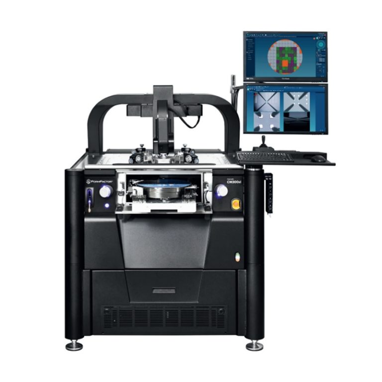
Equipment features: 1. Non-destructive precision testing Micrometer-level probe contact technology...