
A BGA chip is an integrated circuit package with solder balls arranged beneath the package body. Unlike a leaded package, its electrical connections are distributed across the bottom surface. This arrangement supports a higher connection density within a compact footprint, but it also makes PCB routing, soldering and inspection more demanding.
A CSP to BGA adaptor is mainly used when an engineer needs to connect or test a chip-scale package through a different BGA-style footprint. It can support early power-up, firmware bring-up, pin access and functional checks before the final PCB is available.
The adaptor is an engineering bridge, not a production shortcut. Its additional traces, vias, thickness and thermal path can change the test result, especially when the device carries high-speed, analog or heat-sensitive signals.
DEEPETCH works with semiconductor materials, IC substrates, package-related products, chips in stock and custom development. This allows an adaptor discussion to include the package drawing, substrate structure, assembly process and test purpose instead of stopping at the package name.
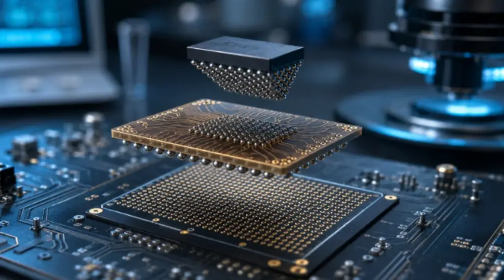
BGA packages are used when a device needs more electrical connections than an edge-leaded package can accommodate efficiently. The solder-ball array provides a compact interface between the package and PCB, but every part of that interface must match the approved drawing.
Each solder ball corresponds to a defined pad or electrical function. During reflow, the balls form solder joints between the package and the PCB.
After assembly, most joints are hidden under the package. A visual check from the side cannot confirm every connection. Depending on the device and risk level, engineers may use X-ray inspection, continuity testing, functional testing and a controlled reflow profile.
The package drawing must identify ball pitch, body outline, orientation and the complete ball map. A mirrored or rotated map can connect a good chip to the wrong PCB nets and make the device appear defective.
BGA distributes connections across the bottom surface rather than only around the package edge. This supports a larger number of signal, power and ground connections without increasing the body outline at the same rate.
The tradeoff appears in PCB routing. Inner rows need escape paths, which can increase layer requirements and place more pressure on via structure, pad design and substrate quality. Package size alone therefore does not determine the total cost of implementation.
Computing, communication and AI-related devices may also require controlled impedance, stable power distribution and an effective thermal path. These requirements should be reviewed together instead of being separated into different purchasing conversations.
Typical problems include open joints, solder bridges, voids, package warpage, incorrect orientation, weak thermal contact and damage caused by an unsuitable reflow process.
Some failures are intermittent. A joint may pass a room-temperature functional check and then open after heating, cooling or mechanical movement. This is why a short power-up test cannot replace assembly and reliability validation.
An adaptor or test fixture can help isolate whether a problem comes from the chip, footprint, PCB or firmware. However, the fixture must be documented carefully enough that it does not introduce a new source of uncertainty.
CSP keeps the package dimensions close to the die size. That is useful when space is limited, but the fine pitch and compact layout may not match the available evaluation board, socket or test platform.
A CSP to BGA adaptor converts the required connections into a footprint that the engineer can access more easily.
The CSP and target BGA footprint may differ in pitch, body size, pad arrangement, orientation and electrical mapping. The adaptor must convert these differences without changing the intended connection.
The supplier should receive the official package drawing and the target board footprint. Screenshots or handwritten maps are not sufficient for release because they may omit no-connect pads, exposed areas, orientation marks or drawing revisions.
Power, ground, clock, analog and high-speed nets should be identified separately. These signals may require different routing, via placement or return paths from ordinary control pins.
An adaptor is useful when an engineer needs evidence before paying for another PCB revision. It can support initial power checks, device identification, firmware bring-up, basic interface testing and early thermal observations.
This can shorten the decision cycle when two candidate devices use different packages or when the final PCB is still being designed.
The adaptor should not be treated as proof of final production reliability. The final PCB will have a different stack-up, trace path, power distribution, mechanical support and thermal environment. Those differences become more important as signal speed and device power increase.
An adaptor can show whether the chip powers up, responds to basic commands and performs selected functions through the converted pin map. It can also help engineers locate firmware, mapping or component-selection problems.
It cannot automatically prove final signal margin, thermal performance, solder-joint reliability or long-term operation. Additional traces and vias may add loss, delay, discontinuity or noise. The adaptor may also block or alter the thermal path used in the final assembly.
For high-speed, RF, precision analog or high-temperature applications, the engineer should define which results are preliminary and which require confirmation on the final PCB.
An adaptor is suitable for temporary evaluation. It becomes less suitable when the project needs a production package, controlled high-speed interconnect or a repeatable thermal and mechanical structure.
CSP is appropriate when the product requires a package close to die size and the PCB can support its pad pitch and routing density.
The compact body does not remove the need for escape routing, assembly control or inspection. A smaller outline may demand tighter PCB and process capability.
If the purpose is only to evaluate a CSP device on an existing BGA test platform, an adaptor may still be efficient. If the compact package will enter production, the final board and assembly process should be designed for the CSP directly.
A custom FCCSP Substrate becomes relevant when the production package requires controlled interconnection between a compact flip-chip device and the external board interface.
This is different from adding a laboratory adaptor. The substrate becomes part of the package structure and must address routing density, power distribution, mechanical stability and heat transfer for the intended device.
Buyers should provide the die or package interface, external connection requirement, size envelope, layer constraints and operating conditions. The substrate should be selected from the actual electrical and mechanical requirements, not only from the abbreviation.
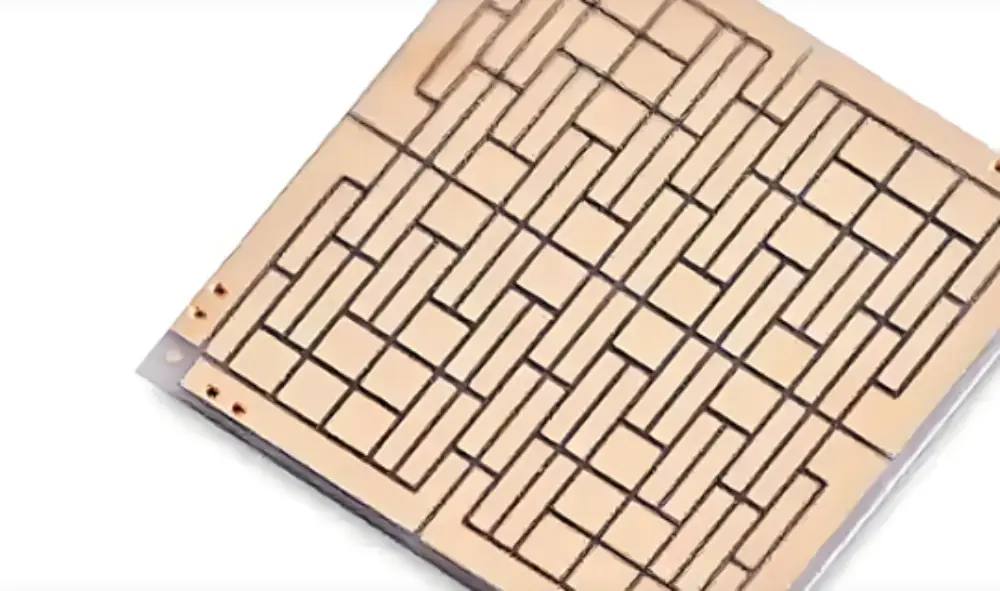
An FCBGA Substrate may be more suitable when the device has a higher I/O count, more complex routing, stronger power-delivery requirements or a larger production package.
This approach is commonly considered for computing, AI and communication applications where substrate structure is part of signal, power and thermal design.
Engineers comparing assembly and inspection requirements across package families can also review SOP vs SOIC Packaging Types. The comparison reinforces a broader procurement rule: package form affects footprint design, assembly, inspection and rework.
A reliable adaptor order begins with controlled technical inputs. The supplier should not need to infer orientation, mapping or test conditions from an incomplete inquiry.
Provide the chip datasheet, official package drawing, ball or pad map, target BGA footprint and the purpose of the test. Record the source and revision of every drawing.
The released adaptor drawing should show the CSP-side pad map, BGA-side ball map, pitch, body outline, finished thickness, orientation mark and total assembled height. It should also show how top-view and bottom-view drawings have been converted.
Identify power, ground, sensitive analog, clock and high-speed nets. If length, impedance or current limits apply, place them in the drawing or engineering notes.
Define how heat leaves the chip during testing and whether the adaptor changes the intended contact with a heat sink, thermal pad or test fixture.
Flatness and warpage should be checked because uneven contact can create weak solder joints or unreliable socket pressure. Inspection may include dimensional checks, continuity testing, open/short testing, visual inspection and X-ray where the assembly risk justifies it.
For projects evaluating package housing and thermal behavior, Ceramic Ball Array Housing CBGA may be relevant when ceramic construction, mechanical stability or high-temperature performance forms part of the design review.
Each inspection record should identify the drawing revision, order or batch, continuity result, dimensional result, orientation check and inspection status.
The supplier should ask what the adaptor is expected to prove. A board intended for basic power-up does not need the same controls as one used for high-speed signal evaluation.
If chip availability is part of the schedule, DEEPETCH’s chips in stock resources can help buyers begin with devices that are available for sampling.
For custom projects, submit the package drawing, target footprint, signal requirements, thermal notes, test objective, quantity and required delivery stage through the DEEPETCH contact page. Resolving a mapping or drawing conflict before fabrication is faster than investigating a failed adaptor after assembly.
A BGA chip uses solder balls beneath the package to support dense electrical connections in a compact area. A CSP to BGA adaptor allows engineers to evaluate a chip-scale package through a different BGA-style footprint when the final PCB is unavailable or does not match.
Use an adaptor for controlled prototype work, early power-up, firmware bring-up and functional checks. Do not use it as automatic proof of final signal integrity, thermal performance or production reliability.
Before ordering, confirm the package drawing, mapping direction, pitch, orientation, target footprint, critical nets, thermal path, inspection method and test objective. If the project requires a repeatable production package rather than a temporary test bridge, review whether an FCCSP or FCBGA substrate is the more appropriate path.
Not by default. BGA can support higher connection density and more routing space, while CSP is useful when the package must remain close to die size. The correct choice depends on PCB space, I/O count, routing, assembly and thermal requirements.
Usually not. It is mainly used for evaluation, testing and prototype work. Final production should be based on a PCB or package structure qualified for the real electrical, thermal and mechanical environment.
Prepare the chip datasheet, package drawing, pad or ball map, target BGA footprint, orientation convention, test objective, signal-speed requirements, thermal notes, expected quantity and required delivery stage.

The DE-CW-1310 DFB EPI wafer, a high-performance epitaxial structure designed for distributed feedback (DFB) lasers operating at 1310 nm....

Ceramic thin-filmvacuum sensor Optical gas massflowmeter Liquid mass flowmeter Force sensor MEMS...

Photoelectric sensing chip Light source chips Optical transmission and modulationchips Optical detection and receptionchips...

Using a“Detach Core”which has two-layers carrier foil structure on the surface as a core, and forming...

Tenting process is a kind of subtractive process, the process as follows: Laminating photosensitive film...

Modified Semi-Added Process abbreviated as mSAP, which can be used on the core or build-up layers, pattern...

Semi-Added Process abbreviated as SAP, using on the build-up-layer pattern forming as follow:First depositing...

The product generally adopts the pressing lamination process of semi-curing sheets , and line formation...

The products generally adopt the Build-up Film Lamination process, and the circuit formation uses the...
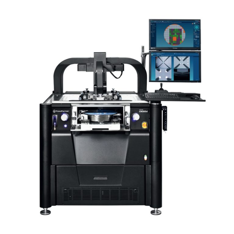
Equipment features: 1. Non-destructive precision testing Micrometer-level probe contact technology...