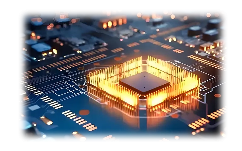
As the semiconductor field moves to better nodes, mixed integration, and fast applications, the work of main equipment parts has turned into a key point for making efficiency and product success. From front-end wafer work to back-end packing and checks, each tiny shift in part action can affect cost, work level, and output speed.
In this setting, picking semiconductor equipment main parts based on exact technical details is not an option. It is a must. This piece looks at the main needs you should think about for different key parts. It also shows how fitting these to your steps leads to the best making results.
For people looking for a reliable helper in exact part building, DEEPETCH gives a full set of answers. As a tech company in Shenzhen started in 2019, DEEPETCH has grown into a tech firm that mixes research, building, making, and selling. Its skills cover power semiconductors, sensors, analog ICs, and others.
The semiconductor equipment field is changing fast. It faces pushes from smaller sizes, more power in small spaces, and harder mixing. This change asks that each main part hits tough technical limits for rightness, heat steadiness, and trust.
Semiconductor raw stuff is a needed part in finishing the semiconductor chain. It helps every step in making semiconductor chips. But it is not just the raw stuff. It is also the built parts. Things like chucks, ion grids, and quartz plates directly touch success rates and work exactness.
This piece will aid you in lining up technical needs with equipment wants. It also brings in DEEPETCH as a special seller of made-to-order semiconductor equipment parts. They offer full steps from building to after-sell help.
Choosing the best main parts rests on knowing each one’s job role and work measures. Here is a simple split by kind:
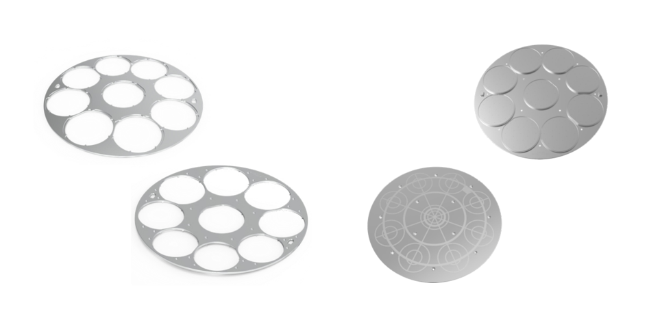
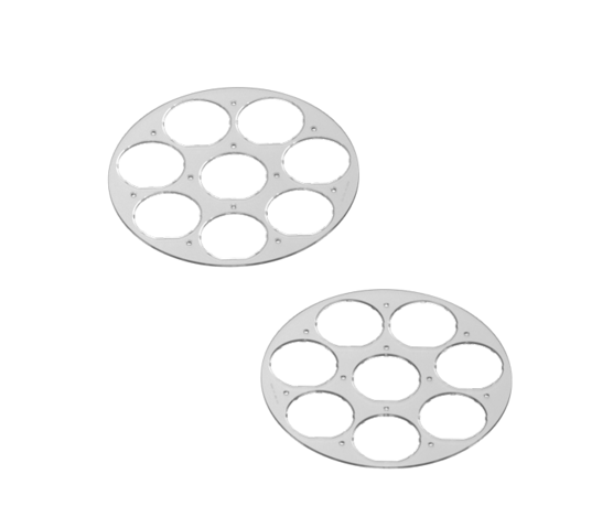
Wafer trays are critical carriers for safely transporting and precisely positioning wafers between processes, especially in PSS nano-imprint lithography for LED sapphire substrates.
Ion source grids right away shape ion planting quality.
Quartz is a must in light and heat steps.
Chip stages must let exact moves and steadiness under changing weights.
To make output lines better, your pick must fit both step-by-step needs and wider field marks:
When you work with DEEPETCH, you get more than just pieces. You reach a full building system:
The work of semiconductor equipment ties close to the technical details of its main parts. This goes from even heat to tiny placing. Picking parts that hit these tough details makes sure step steadiness and making success. Working with partners like DEEPETCH can raise your making skills a lot. They give building-to-send made work backed by field papers.
Q1: How do I determine which technical parameters are most critical for my application?
A: Begin by mapping your process flow (e.g., lithography, etching) to the job needs of each part. Then check SEMI marks. Work with sellers like DEEPETCH who give detail-match help.
Q2: Why is aperture precision important in ion source grids?
A: It makes sure the ion beam shape stays steady in planting. This touches dose evenness and device work.
Q3: Can DEEPETCH support custom sample development before mass production?
A: Yes. Their made process has sample making, testing, feedback get, and last check before big making.
Q4: Are DEEPETCH’s products compliant with global quality standards?
A: Yes. They use ISO9001 watch systems. Plus, 100% test on all send products to make sure trust.

The DE-CW-1310 DFB EPI wafer, a high-performance epitaxial structure designed for distributed feedback (DFB) lasers operating at 1310 nm....

Ceramic thin-filmvacuum sensor Optical gas massflowmeter Liquid mass flowmeter Force sensor MEMS...

Photoelectric sensing chip Light source chips Optical transmission and modulationchips Optical detection and receptionchips...

Using a“Detach Core”which has two-layers carrier foil structure on the surface as a core, and forming...

Tenting process is a kind of subtractive process, the process as follows: Laminating photosensitive film...

Modified Semi-Added Process abbreviated as mSAP, which can be used on the core or build-up layers, pattern...

Semi-Added Process abbreviated as SAP, using on the build-up-layer pattern forming as follow:First depositing...

The product generally adopts the pressing lamination process of semi-curing sheets , and line formation...

The products generally adopt the Build-up Film Lamination process, and the circuit formation uses the...

Equipment features: 1. Non-destructive precision testing Micrometer-level probe contact technology...