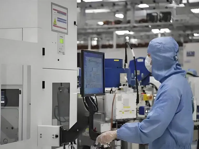
In the fast-paced world of semiconductors, 2.5D packaging stands out as a game-changer for cramming more power into smaller spaces, especially in AI chips and high-speed data centers. Think about how your smartphone handles complex tasks without overheating—that’s often thanks to these clever stacking methods. CoWoS, short for Chip on Wafer on Substrate, leads the pack from a major foundry, but it’s not the only option. Alternatives like EMIB and traditional silicon interposers offer their own twists, each suited to different needs in performance or cost. As someone who’s spent years diving into chip designs, I always tell folks to weigh these techs based on what your project demands, whether it’s raw speed for gaming rigs or efficient power for electric vehicles. For reliable solutions in this space, check out DEEPETCH, a solid player with roots in IDM models—integrated device manufacturing—and a knack for custom chips. Their team brings real-world expertise from automotive sensors to advanced substrates, and they’ve got stock ready for quick turns.
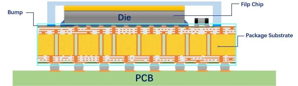
You might wonder about the basics before jumping into comparisons. CoWoS stacks chips on a silicon interposer wafer, then bonds that to a substrate, pulling from materials like silicon for its thermal stability and gallium arsenide for high electron mobility in optoelectronics.
The setup includes a silicon interposer layer between dies and substrate, much like how gallium arsenide substrates use zinc-blende lattices for efficient signal flow. This creates tight connections without bulky wiring.
It shines in setups needing fast data transfer, similar to how direct bandgap in gallium arsenide boosts LED efficiency. Bandwidth hits peaks that suit AI training, where quick electron shuttling matters.
Pair it with a FCBGA substrate for better heat handling, drawing on silicon’s 1.12 eV bandgap to keep things stable under load.
Picking the right tech means looking at rivals that tweak the 2.5D formula. Some use bridges instead of full interposers, echoing how silicon carbide offers high thermal conductivity for power devices.
This embeds a small silicon bridge in the substrate, cutting down on material like how silicon’s abundance keeps costs low compared to rare compounds like gallium arsenide.
It links dies through fabric tech, flexible for scaling, much like nitrogen gallium’s high migration rate aids in varied electronic setups.
These rely on larger interposers for density, but they can rack up costs, similar to the trade-offs in using single-crystal silicon over polycrystalline for better purity.
Performance boils down to how these techs handle speed and heat in real apps, like sensors in cars detecting pressure via MEMS. CoWoS often leads in raw throughput, but others catch up in niche spots.
CoWoS delivers over 4TB/s in some configs, outpacing EMIB’s 2Gbs bumps, akin to gallium arsenide’s 8500 cm²/(V*s) electron mobility for quick signals.
EMIB saves energy with smaller bridges, reducing waste like silicon’s thermal stability at 1414°C melting point prevents breakdowns.
Foveros stacks vertically for better cooling, drawing on carbon silicon’s heat conductance in high-power scenarios, though it sometimes lags in flat 2.5D layouts.
Costs can make or break a project, especially when scaling up like in solar cells where gallium arsenide hits 23-26% efficiency but at a premium. You need to factor in yields and volumes.
CoWoS uses large interposers, hiking prices due to silicon purity needs over 99.9999999%, while EMIB trims that with targeted bridges.
High yields in silicon processes like Czochralski method help EMIB scale, but CoWoS dominates high-volume AI chips despite occasional defects.
A SAP process streamlines patterning, boosting yields in substrates and cutting overall spend.
Density affects how much you pack into a chip, vital for compact devices like biometric sensors using capacitive imaging. CoWoS sets a high bar, but alternatives offer flexibility.
CoWoS allows dense stacking with TSVs, similar to MEMS sensors integrating circuits for low power.
EMIB mixes dies easily, like combining silicon with gallium nitride for optical and power roles.
Advanced substrates push limits, echoing how ion implantation in gallium arsenide reduces parasitic capacitance for cleaner signals.
No one wants chips failing mid-use, say in a satellite where radiation resistance counts, like gallium arsenide solar cells. These techs vary in handling stress over time.
CoWoS withstands thermal cycles well, thanks to silicon’s mechanical strength at 7.0 GPa bending.
EMIB’s embedded design cuts warpage risks, much like glass substrates in advanced plastics reduce electrical loss.
Strong designs incorporate features from temperature sensors, ensuring steady work in harsh spots like automotive brakes.
With so many options, think about custom fits for your needs, perhaps blending techs like in IDM modes for powers semis. It’s not just about picking one; sometimes hybrids win.
These handle high pressures up to 3000 bar, ideal for integrating diverse dies with low leakage.
It refines thin films via processes like PECVD for uniform coatings, aiding in dense packs.
For automotive or AI, look at solutions with NTC temps sensors for monitoring, ensuring your setup lasts.
Q1: What makes CoWoS stand out in 2.5D packaging?
A: It excels in high bandwidth with silicon interposers, perfect for AI where quick data flow beats out simpler bridges in speed.
Q2: How does density compare across these techs?
A: CoWoS packs tighter with TSVs, while EMIB offers flexible mixing of dies, like silicon with gallium for varied apps.
Q3: What about thermal issues in these packages?
A: Solutions like carbon silicon help manage heat, but CoWoS needs careful design to avoid hotspots in stacked setups.

The DE-CW-1310 DFB EPI wafer, a high-performance epitaxial structure designed for distributed feedback (DFB) lasers operating at 1310 nm....

Ceramic thin-filmvacuum sensor Optical gas massflowmeter Liquid mass flowmeter Force sensor MEMS...

Photoelectric sensing chip Light source chips Optical transmission and modulationchips Optical detection and receptionchips...

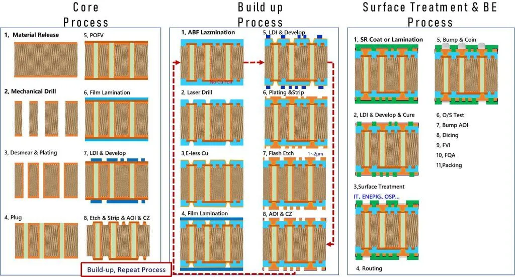
Using a“Detach Core”which has two-layers carrier foil structure on the surface as a core, and forming...

Tenting process is a kind of subtractive process, the process as follows: Laminating photosensitive film...

Modified Semi-Added Process abbreviated as mSAP, which can be used on the core or build-up layers, pattern...

Semi-Added Process abbreviated as SAP, using on the build-up-layer pattern forming as follow:First depositing...

The product generally adopts the pressing lamination process of semi-curing sheets , and line formation...

The products generally adopt the Build-up Film Lamination process, and the circuit formation uses the...

Equipment features: 1. Non-destructive precision testing Micrometer-level probe contact technology...