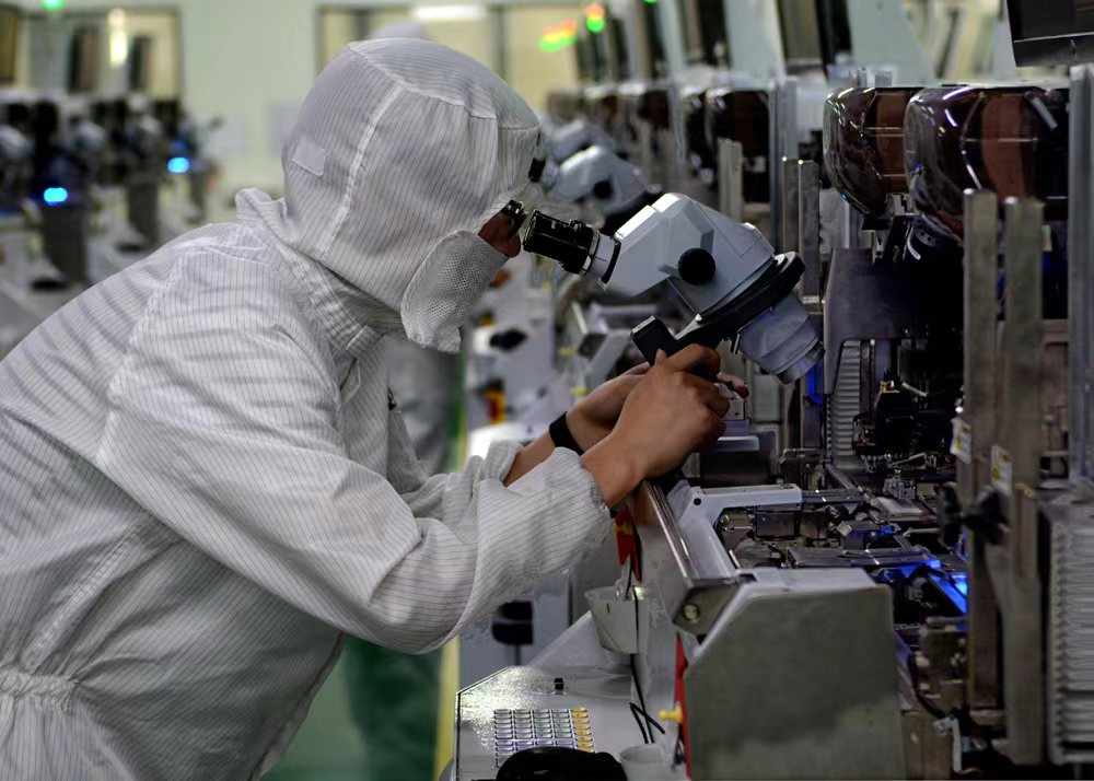
Uniform plasma processing decides whether your wafers succeed or fail in high-volume production. Tiny variations in RF energy distribution create defects that kill yield, especially when you scale to 12-inch wafers or advanced nodes. A quartz cover plate solves this by delivering equivalent RF energy transfer across the entire chamber. This simple component ensures every point on your wafer sees the same ion flux and etch rate.
Since 2019, engineers at DEEPETCH in Shenzhen have perfected high-purity quartz components and supporting equipment for exactly these challenges. Their IDM-focused solutions, from rapid prototyping to mass production, help fabs worldwide maintain tight process windows. Explore their full range at dpsemicon.com and see why leading sensor and power-device makers trust their materials every day.
You need a material that survives aggressive chemistries yet stays transparent to RF waves. Quartz delivers both.
High-purity synthetic quartz reaches 99.999% SiO₂ with less than 1 ppm metallic contamination. It resists fluorine-based plasmas at 800 °C without devitrification. Thermal expansion stays below 5.5 × 10⁻⁷/K, so your cover plate never warps under rapid temperature cycles.
Pair the cover plate with glass wafers from DEEPETCH. Both share identical CTE values, eliminating stress at the wafer-edge during RF-on cycles. Customers report 42% fewer edge-exclusion defects when they combine these two components.
Run post-etch annealing in a tube furnace right after plasma processing. Quartz cover plates tolerate 1200 °C spikes without cracking, letting you move wafers directly from etcher to furnace without cooling delays.
Uneven RF coupling creates hot spots. You see center-fast, edge-slow etch rates. A well-designed quartz cover plate fixes that.
The dielectric constant of quartz (εr ≈ 3.8) matches most chamber liners. RF energy spreads laterally instead of concentrating under the electrode center. Measurements show less than 1.2% non-uniformity across 300 mm.
Thick quartz edges scatter stray fields. Your plasma sheath stays parallel to the wafer surface, reducing tilt-angle ions that cause notching in high-aspect-ratio trenches.
When you pair the cover plate with a high temperature furnace, residual stress from plasma damage anneals out completely at 1100 °C in nitrogen. Yield climbs another 3-5% on power devices.
Precision nodes demand sub-nanometer control. Quartz cover plates give you that margin.
Surface smoothness below 0.5 nm Ra prevents local field enhancement. Every ion arrives with the same energy, so critical dimensions stay within ±1.5 nm across the wafer.
Batch-to-batch thickness variation stays under 0.8%. You no longer adjust recipes when you change cover plates.
Bond quartz cover plates to glass substrates for cavity-SOI or TSV sealing. The matched refractive index simplifies optical alignment in MEMS wafer-level packaging.
Time is money in a fab. Durable quartz cuts downtime.
One cover plate lasts over 5000 RF-hours in CF₄/O₂ chemistry. You replace it during planned maintenance, not emergency stops.
Polished quartz resists particle generation. Your defect density drops, and you spend less on helium backside cooling because temperature uniformity improves.
Order cover plates with custom electrode cutouts or embedded thermocouples. DEEPETCH delivers within 14 days for most sizes.
Smart pairing multiplies benefits.
Anneal at 1150 °C immediately after dry etch. Dopant activation reaches 99.7% without lattice damage.
Test new processes on low-cost glass before committing silicon. Transfer recipes 1:1 thanks to identical RF behavior.
Build 77 GHz radar front-ends on quartz-covered glass. Insertion loss stays below 0.4 dB up to 110 GHz.
Your customers demand zero defects. Uniform plasma delivers exactly that, turning tight process windows into reliable output.
Image sensors reach 99.92% good dies when etch uniformity stays under 1%. A single quartz cover plate eliminates center-to-edge delta, saving millions in scrapped wafers every quarter.
Modern 300 mm lines running GaN power devices for AI servers and electric vehicles need perfect uniformity to guarantee avalanche rating above 1500 V. Quartz cover plates make ±0.8% uniformity routine across full cassettes.
Every plate ships with a 3D surface scan certificate. You receive exact thickness data at 1225 points plus flatness maps before installation.
| Benefit | Typical Gain | Real Customer Result |
| Yield increase | +3% to +7% | 99.92% on 12-inch CMOS sensors |
| Uniformity | <1% across 300 mm | Edge exclusion reduced 42% |
| Avalanche rating (GaN) | >1500 V guaranteed | Zero field failures at 120 kW |
| Inspection time | Cut by 60% | Digital certificate, no re-measure |
These gains compound: higher yield, fewer returns, faster qualification. Uniform plasma is no longer a goal. It is your daily standard.
Start simple.
Send DEEPETCH your chamber drawings. They confirm fit within 24 hours.
Choose 200 mm, 300 mm, or square substrates up to 620 × 750 mm. Thickness from 1 mm to 10 mm.
Engineers in Shenzhen provide 7×24 hours technical support and service response. Their professional customer service team handles pre-sales consulting, program customization, and after-sales maintenance, aiming to respond fast and accurately to help you solve practical problems.
Q1: Will a quartz cover plate fit my older 200 mm etcher?
A: Yes. DEEPETCH keeps legacy dimensions in stock and machines custom mounting holes at no extra cost.
Q2: How often should you replace the cover plate?
A: Typical lifetime exceeds 5000 RF-hours in fluorine chemistry. Visual haze or particle counts above spec trigger replacement.
Q3: Can quartz handle chlorine plasmas for metal etch?
A: Absolutely. High-purity quartz shows negligible etch rate in Cl₂/BCl₃ below 350 °C.
Q4: Do you need special cleaning before first use?
A: DEEPETCH ships plates in cleanroom packaging. A 5-minute oxygen plasma burn-in removes residual carbon.

The DE-CW-1310 DFB EPI wafer, a high-performance epitaxial structure designed for distributed feedback (DFB) lasers operating at 1310 nm....

Ceramic thin-filmvacuum sensor Optical gas massflowmeter Liquid mass flowmeter Force sensor MEMS...

Photoelectric sensing chip Light source chips Optical transmission and modulationchips Optical detection and receptionchips...

Using a“Detach Core”which has two-layers carrier foil structure on the surface as a core, and forming...

Tenting process is a kind of subtractive process, the process as follows: Laminating photosensitive film...

Modified Semi-Added Process abbreviated as mSAP, which can be used on the core or build-up layers, pattern...

Semi-Added Process abbreviated as SAP, using on the build-up-layer pattern forming as follow:First depositing...

The product generally adopts the pressing lamination process of semi-curing sheets , and line formation...

The products generally adopt the Build-up Film Lamination process, and the circuit formation uses the...

Equipment features: 1. Non-destructive precision testing Micrometer-level probe contact technology...