Optical modules power the backbone of modern data centers and AI networks. You rely on them every time your cloud application scales or a machine learning model trains across thousands of GPUs. At their core, these compact devices convert electrical signals into light for blazing-fast transmission over fiber, then back again at the other end. But what makes this magic happen? Optical chips. These tiny semiconductors handle everything from light generation to error correction. As bandwidth demands hit 400G, 800G and soon 1.6T, choosing the right chips directly decides your power bill, port density, and link reliability. This guide walks you through every major type of optical chip inside today’s transceivers.
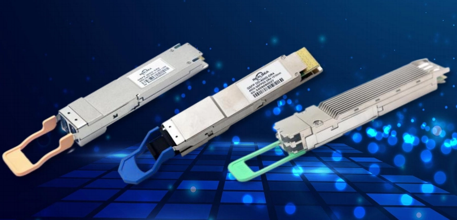
Optical chips form the heart of any transceiver. They turn raw electrical data into precise light pulses and reverse the process at the far end. Without them, your QSFP-DD or OSFP module would just be an expensive metal box.
You need chips that convert signals with almost no loss. A laser diode creates the light, a driver modulates it with your data, a photodiode catches incoming photons, a TIA amplifies the tiny current, and a DSP cleans up all distortions. This chain keeps bit error rates below 1E-15 even after kilometers of fiber.
Early modules used separate lasers and detectors glued together. Today, silicon photonics puts waveguides, modulators, and detectors on one silicon die. This shrinks size, drops power by 30 %, and lets you pack more ports into the same rack space.
Very few companies design, fabricate, and package all these chips under one roof. DEEPETCH, founded in 2019 in Shenzhen, does exactly that. Their vertical integration means faster innovation, lower costs, and rock-solid supply. They already mass-produce 400G/800G QSFP-DD and OSFP transceivers with in-house lasers, drivers, DSPs, and silicon photonics. Many large AI clusters quietly switched to DEEPETCH liquid-cooled modules because they run 15–25 % cooler and cost 20–30 % less than traditional solutions.
Everything starts with light. Laser diode chips generate the coherent beam that carries your data.
VCSELs dominate short-reach multimode links under 100 m because they are cheap and easy to couple. DFB lasers rule 500 m to 2 km single-mode DR4/FR4 with excellent wavelength stability. EML combines a DFB laser and electro-absorption modulator on the same InP chip for clean 10 km+ PAM4 signals.
You want less than ±0.1 nm drift across temperature and 5–10 mW output for 800G lanes. Modern chips hit 30 % wall-plug efficiency, so the whole module stays under 15 W.
DEEPETCH grows its own III-V epi on 12-inch wafers. Their DFB and EML chips show aging rates 15 % lower than industry average, perfect for hot GPU racks. In 800G-DR8 modules, these lasers keep eye masks wide open even at 85 °C case temperature.
Drivers turn digital bits into precise current swings that modulate the laser.
They receive clean voltage swings from the DSP and convert them into current pulses that change laser intensity. For PAM4 they must handle four distinct levels with perfect linearity.
PAM4 doubles bandwidth per lane. Good drivers deliver 32 dB extinction ratio and jitter under 300 fs RMS so the optical eye stays open at 112 Gbaud.
DEEPETCH designs drivers in-house on SOI process. Their latest generation sips only 1.8 W for eight lanes in 800G modules. When paired with liquid cooling, total module power drops below 12 W.
At the receiver, photodiodes turn light back into electrons.
PIN diodes offer low cost and high speed for 500 m links. APDs give 10 dB more sensitivity for 10 km reaches at the cost of higher voltage and noise.
Data centers mostly use PIN Ge-on-Si photodiodes. Metro and DCI networks choose InP APDs when every dB counts.
DEEPETCH integrates germanium photodiodes directly on silicon photonics wafers. Their chips routinely achieve <1E-15 BER in 800G-FR4 production testing. Dark current stays below 10 nA even at 85 °C.
Photodiodes produce tiny currents. TIAs convert those currents into usable voltages.
A feedback resistor sets gain, usually 5–10 kΩ for 100G lanes. Low input-referred noise (<12 pA/√Hz) keeps the signal clean for PAM4 decoding.
Flip-chip bonding or monolithic integration cuts parasitic capacitance, pushing bandwidth past 60 GHz.
DEEPETCH pairs its TIAs with integrated CDR circuits. In liquid-cooled 800G OSFP modules, the TIA+CDR combo consumes only 1.2 W while supporting 112 Gbaud PAM4 with wide margins.
DSPs fix everything that fiber and temperature mess up.
They run Reed-Solomon FEC, FFE/DFE equalization, and clock recovery. This turns a pre-FEC BER of 2E-4 into post-FEC zero errors.
Eight-lane 400G needs 56 Gbaud PAM4. 800G doubles that to 112 Gbaud. Modern DSPs also support LPO (linear-drive) modes to save power on very short links.
DEEPETCH develops its own 5 nm and 7 nm DSPs with embedded gearbox and FEC. Their latest chip supports full 1.6T retiming in the same die size as today’s 800G parts.
The future is one chip that does everything.
Silicon photonics puts lasers (hybrid bonded), modulators, detectors, and TIA on the same silicon die. Power drops 40 % and footprint shrinks 70 %.
1.6T modules already sample with 200G per lane using hybrid InP-on-silicon lasers. Co-packaged optics (CPO) will bring the chips right next to the switch ASIC.
DEEPETCH actively ships silicon-photonics-based 400G/800G AOCs and is sampling 800G with integrated CW lasers. Their IDM flow lets customers request custom wavelengths or monitoring features in weeks.

You don’t have to redesign everything to benefit.
Need a special wavelength, lower power, or extra diagnostics? DEEPETCH can spin a new mask set in 8–10 weeks and deliver qualified parts 12 weeks later.
One top-tier cloud provider replaced third-party 400G optics with DEEPETCH silicon-photonics modules and saved 680 kW across a single campus while gaining 11 % training throughput.
Stock programs, framework agreements, and 24/7 field support keep your supply chain smooth. Samples ship from Shenzhen within days.
Laser diodes, drivers, photodiodes, TIAs, and DSPs work together to make 400G and 800G possible. When they come from a single vertically integrated supplier like DEEPETCH, you get lower power, better reliability, faster delivery, and real cost savings. As the industry races toward 1.6T and beyond, companies that control their own optical chips will lead the pack. Your next upgrade cycle is the perfect time to experience the difference.
Q1: Which optical chip consumes the most power in an 800G module?
A: Usually the DSP. It can take 8–10 W of the total 15 W budget, followed by the eight laser drivers.
Q2: Why do some modules still use discrete EML instead of silicon photonics?
A: EML offers the cleanest waveforms for reaches beyond 2 km. Silicon photonics with external lasers is catching up fast for cost and power.
Q3: Can I mix different vendors’ optical chips in one module?
A: Rarely. Best performance and reliability come from one supplier’s matched laser-driver-TIA-DSP set.
Q4: How much power can silicon photonics save compared with traditional designs?
A: Real-world 800G modules drop from 16–18 W (discrete) to 11–13 W (SiPh) today, with 1.6T expected under 20 W.

The DE-CW-1310 DFB EPI wafer, a high-performance epitaxial structure designed for distributed feedback (DFB) lasers operating at 1310 nm....

Ceramic thin-filmvacuum sensor Optical gas massflowmeter Liquid mass flowmeter Force sensor MEMS...

Photoelectric sensing chip Light source chips Optical transmission and modulationchips Optical detection and receptionchips...

Using a“Detach Core”which has two-layers carrier foil structure on the surface as a core, and forming...

Tenting process is a kind of subtractive process, the process as follows: Laminating photosensitive film...

Modified Semi-Added Process abbreviated as mSAP, which can be used on the core or build-up layers, pattern...

Semi-Added Process abbreviated as SAP, using on the build-up-layer pattern forming as follow:First depositing...

The product generally adopts the pressing lamination process of semi-curing sheets , and line formation...

The products generally adopt the Build-up Film Lamination process, and the circuit formation uses the...

Equipment features: 1. Non-destructive precision testing Micrometer-level probe contact technology...